
How to Cascade Shift Registers
In this project, we are going to cascade 2 shift registers together using the 74HC595 shift register.
This means that we pretty connect them together, so that instead of controlling 8 outputs, the cascaded shift registers can now control 16 outputs.
You can cascade as many shift registers as you want. If you want to cascade a third one, it can control 24 outputs. If you cascade a fourth shift register, it can control 32 outputs.
But in this circuit, we will cascade an additional shift register, having 2 in total.
Cascading shift registers is very simple once you know how to do it, because the 74HC595 is purposely designed to be able to add additional shift registers. So once you simply how to connect it, it's very simple.
As stated, the advantage is that we can control many more outputs. We will add 2, so we can control 16 outputs. This means we can simultaneously shift 16 bits.
Be prepared to a have a lot of resistors and LEDs for this project, because you'll
need 16 of each.
Components
- 74HC595 Shift Register
- 16 LEDs
- 16 220Ω resistors
- Arduino
The 74HC595 shift register is one of the most popular and widely used ones in the electronics industry. One individual 74HC595 can control 8 outputs. This means it can control, for example, 8 LEDs.
The shift register, in total, has 16 pins.
The pinout for the shift register is shown below.
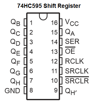
The table below summarizes these pin connections.
| Pin | Description | Function |
| QA-QH | Output pins | Outputs of the shift register |
| VCC (Pin 16) | Power | Positive voltage for the shift register |
| GND (Pin 8) | Power | Ground for the shift register |
| QH' (Pin 9) | Serial Out | Serial out is used to shift data to another 74HC595 shift register |
| Master Reclear, active low | This sets all the bits in the shift register to 0 or off if pulled LOW. | |
| Shift Clock (Pin 11) | Shift Register Clock Pin | If pulled HIGH, this shifts all the values in the shift register forward one. |
| Latch Clock (Pin 12) | Stroage Register Lock Pin | When pulled HIGH, it outputs the new shift register values. |
| Output enable, active low | This enables the output when grounded and disables it when high. | |
| Serial Data Input (Pin 14) | Input for New Serial Data | This is the input pin for the new serial data. |
The 74HC595 shift register has 8 outputs. This means you can connect up to 8 output devices, such as LEDs or buzzers, to the shift register. The output pins are QA-QH, 8 in total. QA, pin 15, is the first output pin. Next are QB-QH, which are pins 1-7. These output pins do not connect to the arduino microcontroller. Instead, the outputs, which in this case are LEDs, are connected to them.
To provide power to the 74HC595 shift register, we give +5V to VCC and we connect GND to ground on the arduino microcontroller.
When connecting shift registers to microcontrollers, the serial data input line (pin 14) gets connected to digital pin 11 on the arduino. Through this connection, through our code, we will write the data that we want to be displayed at the output. For example, we may write 11111111 to the serial data line. If this done while the clock is HIGH, then the 1s will be shifted into the storage register. Now the storage register will read 11111111. Once we do the next step, latch it, which means we transfer the data from the storage register into the outputs, it will show up at the output. This means the LEDs will all turn on.
The clock pin (pin 11), is the clock for the shift register. The 74HC595 is clock-driven on the rising edge. This means that in order to shift bits into the storage register of the shift register, the clock must be high. And bits are transferred in on the rising edge of the clock. So the clock must be HIGH when new data is being driven into the storage register.
The latch pin (pin 12) is a very important pin. This pin takes the data that is stored in the storage register and when driven HIGH, transfers the data to the output. So when we initially transfer in data, it goes into the storage register but does not show up at the output. It only shows up at the output when the latch pin is HIGH. This is when we then we see the LEDs turn on. So the latch pin can be seen as like the final step in the process to seeing our results at the output, which in this case are LEDs.
The CLEAR pin is an active low pin. This means that when it is grounded, all data in the storage register is cleared to 0. In order for this not to happen, we keep it at HIGH, so we connect it to VCC.
The Output Enable pin allows us to turn on or off all the outputs. Usually, we want this enabled so that there can changes on the output side. If this is disabled, then no output can be turned on. This pin is an active low pin, which means when it is grounded, all output pins are disabled. So normally we keep this pin HIGH, so it's tied to VCC.
The QH' pin is the serial data output pin. This is the pin we use to cascade an additional shift register. So instead of being able to switch on 8 outputs, we
can then switch on 16 outputs. How this works is we will take the serial data output pin of the first shift register and connect to the serial data input on the second shift register. This way, the
data from the first shift register feeds directly into the second shift register. This is how the data cascades into the next.
Cascaded Shift Register Circuit
The cascaded shift register circuit we will build with an Arduino is shown
below.
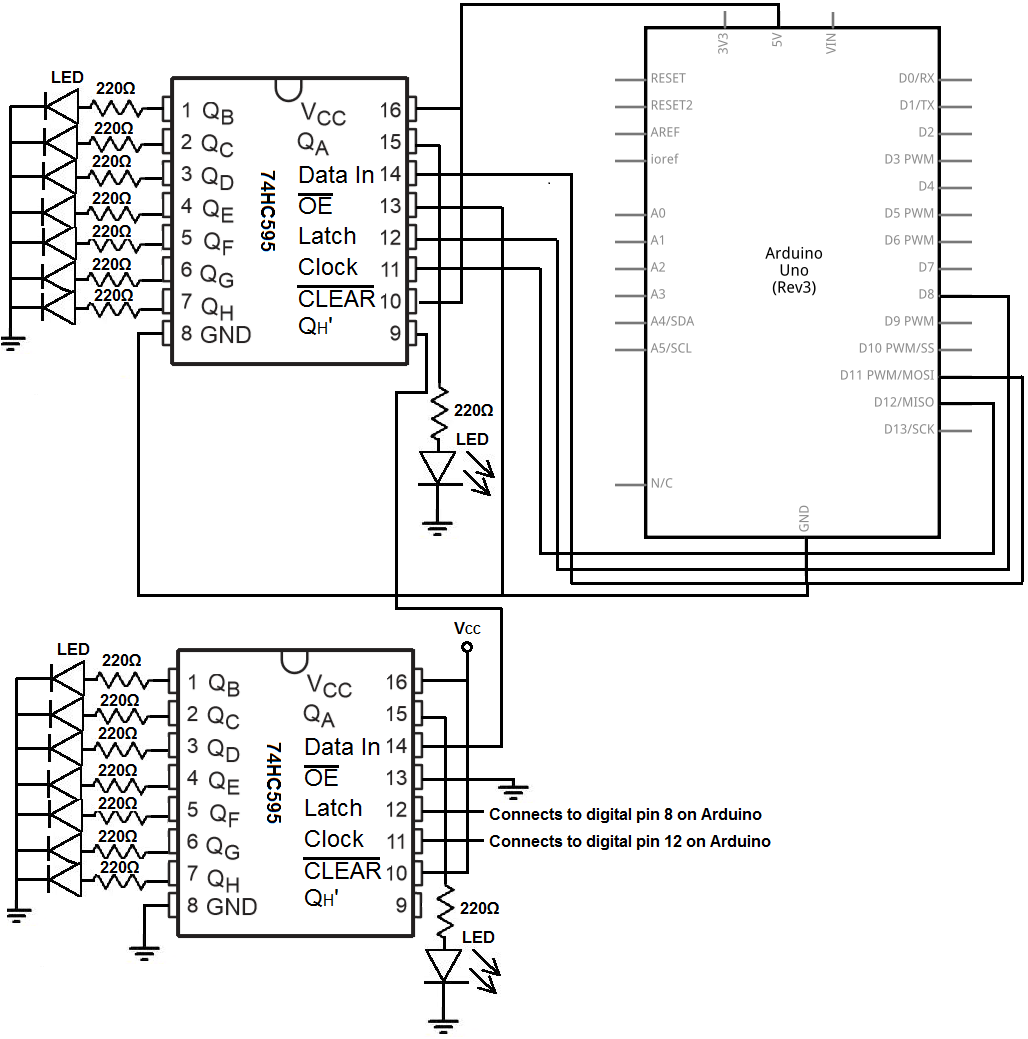
This shift register circuit has pretty basic connections.
First we connect power. So we connect both VCCs of the shift registers to the 5V arduino terminal. We connect the grounds of the shift registers to the GND arduino terminal. This establishes sufficient power for both shift registers.
Next we connect both clock pins (pin 11) to digital pin 12 of the arduino.
We connect the latch pins (pin 12) to digital pin 8 on the arduino.
For the first shift register, we connect the serial data input pin to digital pin 11 on the arduino. The data input on the second shift register will have the serial data output line connected to it. More will be explained below.
Since the Output Enable pin is active low, we connect it to be ground, because we normally want outputs to be enabled. If outputs are disabled, we can't write anything to outputs. Outputs are permanently disabled unless enabled. Since we do not want them disabled ever in this circuit, we simply connect to ground permanently.
Since the CLEAR pin is active low, we connect to VCC, because we don't want the storage register to be cleared normally.
Since we are cascading an additional shift register, for the shift register, we connect the serial data output line to the serial data input line on the second shift register. This allows the data to flow seamlessly from the shift register to the second one.
Lastly, we connect the LEDs to the output pins, QA - QH. To each of the LEDs, we connect a current-limiting 220Ω resistor.
Code
This is the code necessary to run this shift register circuit.
const int latchPin= 8;
const int clockPin=12;
const int dataPin= 11;
void setup() {
pinMode(latchPin, OUTPUT);
pinMode(clockPin, OUTPUT);
pinMode(dataPin, OUTPUT);
Serial.begin(9600);
Serial.println("Enter the number of LEDs you want to turn on from 0-15:");
}
void loop(){
if (Serial.available() > 0) {
//so if a user types in a number from 0 to 9 in ASCII
//simply subtract 48 to get the actual value
int bitDesired= Serial.read() - 48;
registerWrite(bitDesired, HIGH);
}
}
void registerWrite (int PinToSetHigh, int PinState) {
byte bitsToSend= 0;
digitalWrite (latchPin, LOW);
bitWrite(bitsToSend, PinToSetHigh, PinState);
shiftOut(dataPin, clockPin, MSBFIRST, bitsToSend);
digitalWrite(latchPin, HIGH);
}
In the first block of code, we show the connections of the latchPin, clockPin, and dataPin to the arduino board. These all connect to digital pins.
In the second block of code, we set the latchPin, clockPin, and dataPin as outputs. This because the arduino writes to them. If they were inputs, the arduino would read them. We also create a Serial Monitor so that the user can enter from numbers 0-15 the amount of LEDs desired to be turned on.
The next block, our loop() function, reads the value that was entered and writes into the storage register. We then, as the final line, turn the latch Pin HIGH so that the data in the storage register then gets transferred to the output pins. And this is when we see the LEDs turn on. We initially see the numbers light up that we entered into the Serial Monitor. Each the time the loop() function is executed, the bits then shift to the right. The Most Significant Bit (MSB), gets shifted out first. It's a left shift till all the LEDs are shifted out. We then can reset the microcontroller and put in a new value. If you want to left shift, you can change the shiftOut function from MSBFIRST to LSBFIRST. This will shift out the Least Significant Bit (LSB) first.
So this is an example of a cascaded shift register circuit.
Related Resources
How to Build a Shift Register Circuit with an Arduino
How to Build a Shift Register Circuit with Manual Pushbutton Control