
How to Build a D Flip Flop with NAND Gates
In this project, we will show how to build a D flip flop from NAND gates.
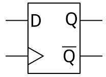
A flip flop is an electronic device that can store bits of information.
A D flip flop stores 2 bits of information at the outputs, Q and
Q and
The D flip flop has a single input. A LOW logic level, or 0, sets Q to 0. A HIGH logic level, or 1, sets Q to 1. Having a 0 at the input "resets", or clears, the value to 0. Having a 1 at the input "sets" the value to 1.
A D flip flop really is a SR flip flop, which is a "set-reset" flip flop. The only difference is that it has an added NOT gate in front of it. This NOT gate prevents the hold condition and the indeterminate condition of the SR flip flop from occurring. The indeterminate condition is an especially troubling state for the SR flip flip because it can produce unpredictable outcomes, which of course would want to be avoided.
We will build a D flip flop from NAND gates. Using a 4011 chip, which contains 4 NAND gates, we can construct
a D flip flop circuit.
Components Needed
- 2 4011 NAND Gate Chips
- 2 LEDs
- 2 470Ω resistors
The 4011 quad NAND gate chip can be obtained very cheaply from a number of online retailers for just a few cents. One place it can be obtained from is Tayda Electronics at the following link: Tayda Electronics- 4011 Quad 2-Input NAND Gate IC. However, it is a very popular chip and many electronics parts suppliers have them.
The pinout of the 4011 is shown below, so that you can see how to connect it in the circuit.
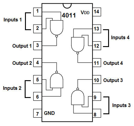
Each NAND gate has 2 input pins and 1 output pin.
We will use 2 pushbuttons as our inputs to the NAND gate.
The values we will use for the pull down resistor is 10KΩ.
The other components we need are the LEDs and the 470Ω resistors in series with the LEDs to limit current to them so that they don't burn out.
A D flip flop is a very simple flip flop. It has only has 1 input. And it has 2 outputs.
The logic table of a D flip flop is shown below.
| D Flip Flop Logic Table | ||
| Input | Q | Q |
| 0 | 0 | 1 |
| 1 | 1 | 0 |
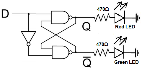
D Flip Flop from NAND Gates (Non-clocked)
The first D flip flop circuit we will build will be an asynchronous, or non-clocked, D flip flop. This flip flop does not have a clock cycle, so it does not execute on a clock timing schedule. It simply executes an instruction whenever it gets the data on the data line.
For very basic applications, this can be sufficient. But for more advanced uses, where you want the input to the D flip flop to work in synchrony with a clock signal, then you would want a synchronous, or clocked, D flip flop circuit.
But for basic demonstration, we show a non-clocked D flip flop below.
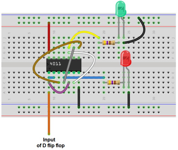
Below is the breadboard schematic version of the above circuit
so that you can see the exact wiring of the circuit to the 4011 chip.
First and foremost, we must give power to the chip. We will feed it 5V of power, so we give +5V to pin 14 and we connect pin 7 to GND. This establishes power to the chip.
On the chip, there are 2 output terminals, Q and
To create the NOT gate, we use a NAND gate. To create a NOT gate with a NAND gate, you simply just connect the 2 inputs of a NAND gate together. Because both inputs are tied together, they have to be the same value. So you either have 2 LOW logic states or 2 HIGH logic states. Since, in NAND gate logic, 2 LOWs give a HIGH as an output and 2 HIGHs as inputs give a LOW as output, it functions as a NOT gate in that it always gives the opposite logic state at the output than what is at the input.
If you were to remove the NOT gate from the circuit, you would have a SR flip flop. The SR flip flop has 2 inputs, not one like the D flip flop. The D flip flop can be seen as an improvement over the SR flip flop, because the SR flip flop can produce an undefined state, when both inputs are HIGH. In this condition, the SR flip flop yields an indeterminate result. The D flip flop makes this impossible because with a D flip flop, there is a NOT gate before all the other gates. This NOT gate makes it impossible for both inputs to be the same value. Thus, we eliminate the indeterminate condition. We also eliminate another condition, called the Hold condition; this is when both inputs are LOW. This condition is less troublesome than the indeterminate condition, but it still is not necessary. Therefore, the D flip flop really is more efficient than the SR flip flop.
When the input is 0 to the flip flop, Q=0 and
When the input is 1 to the flip flop, Q=1 and
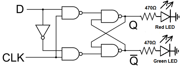
D Flip Flop from NAND Gates (Clocked)
Now, here, we show a synchronous, or clocked, D flip flop. This is the same D flip flop as above, only that it requires a clock signal. The input of the D flip flop works in synchrony with the clock signal.
When the clock signal is HIGH, the data input can be registered in.
When the clock signal is LOW, no input on the data line can be entered in.
Below is the breadboard schematic version of the above circuit.
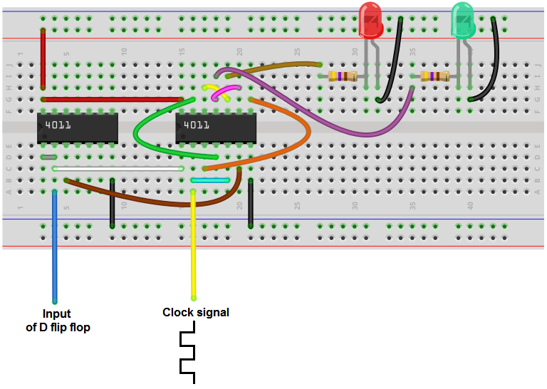
So this circuit is now a clocked D flip flop. As long as the clock signal is
HIGH, it clocks in the data at the input. If the clock is LOW, no new data can be clocked
into the flip flop. It simply will be in a HOLD state when the clock is LOW, meaning
it holds whatever value was in the output previously.
Related Resources
How to Connect a Pull Down Resistor