
EasyEDA Online PCB Layout Sofware

So, in this article, I go over EasyEDA software, which is a type software that you can use in order to build circuit schematics that are able to be converted to PCB format.
PCBs, printed circuit boards, are the standard type of setup used to build real-world electronic devices.
Breadboarding is just for prototyping, while PCBs are for real-world use, when you're actually releasing a product that can be sold in the real world.
EasyEDA software is a unique software that enables you to build a circuit online that can be converted into PCB format automatically. You can then purchase the PCB from this company, and they can deliver you the board. The great thing is, it's free and doesn't require any installation. It can all be done online.
So in this article, I'm specifically going to go over how you can use the EasyEDA software to build a circuit schematic, which can then be converted into a PCB.
So the instructions below have been provided by the site, and I add my own personal comments to it.
PCB Layout Tutorial
In this PCB layout tutorial I hope to tell you how to create a good PCB layout very easily and clearly. I’d like to take EasyEDA PCB design editor as an example because it’s free, easy-to-use and without any installation but it brings you fast PCB design and easier circuit design experience.
Step 1: Convert your schematic to a PCB
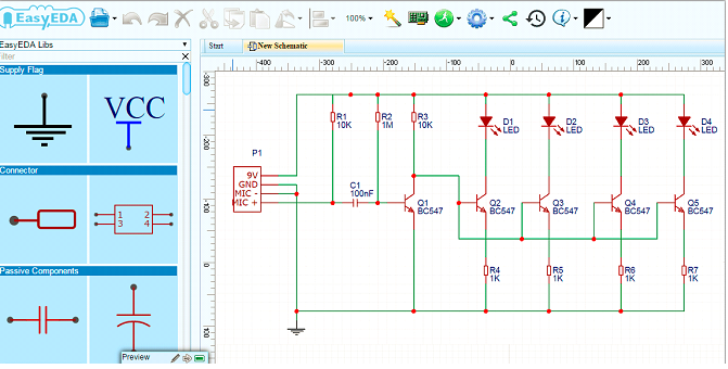
First you could draw your schematic on EasyEDA editor as below image showed. I’m using this music controlled LED’s schematic for this tutorial:
Once you’re finished building the schematic, click on “Convert project to PCB”

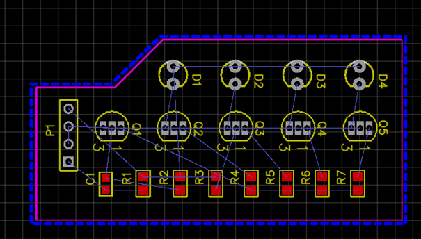
Step 2: Placing the components
Now it’s time to drag and drop the components to the spots where you want them to be. If you want your PCB to look as clean as possible I suggest placing all components with the same function next to each other, like resistors for example. Also make sure to leave some extra space between components, especially capacitors since the size may vary. Apart from the fact that the size may vary leaving some space will make the soldering a lot easier. Especially when you have to solder SMD components.
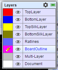
Step 3: Drawing a custom outline
First, select the “BoardOutline” layer in the layers menu:
Click on the current outline (the pink square in your editor) and press delete to get rid of it.
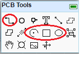
Now you can use the following tools to draw a new outline:
Once you’re done with your outline you can switch back to either the top or bottom layer.
Step 4: Creating a copper area (GND)
A very easy way to connect a lot of parts to a signal (mostly used GND) is to create a copper area.
You can create a copper area by using the tool “Copper Area” in the Tools menu.
Once you’re done drawing just outside of the outline your PCB should look something like this:
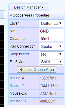
Now click on the dotted line you just drew and check whether these settings are correct. Once they are correct you can click “Rebuild CopperArea” and your PCB will be filled with copper only connecting to GND.
Step 5: Routing
There are 2 different ways to perform this step. The easiest is to use the “Auto Router” function. If you’re creating a PCB where the current is low you can use this method, but if you need different track sizes you’re better off routing the PCB yourself.
The Auto Router function can be found here:

You should see blue lines all over the PCB. These indicate which component’s pin is connected to which pin.
Now use the “Track” tool in the tools menu and click on a pad. Once you move your mouse you should see the blue line moving as well. Make sure not to cross any other tracks or pads and start routing all tracks to the correct pads.
You can switch to the opposite layer (top/bottom) if you have to cross lines. If you have to switch to another layer for a SMD component you have to use a “via” which can also be found in the tools menu. A via is basically a copper connection between multiple layers.
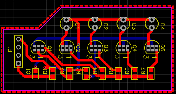
This is an example of what your PCB could look like (With “Fill Style” None in the copper area properties):
Step 6: Adding holes
If you want to mount your PCB onto something, it might be useful to add some holes. Click on the “Hole” tool in the tools menu. Now you can set the size of the hole on the right. Make sure you’re using the right units!! Once the size has been set you can click on the spots you want your holes to be. Don’t place holes onto components or tracks. Resize your PCB outline if you need more space to add the holes.
Step 7: Adding Text and Images
To add text click on the “Text” or “Image” tool in the tools menu. Place the text where you want it to be and change the text in the right properties menu. You can also change the desired layer in the menu.
Step 8: Finalizing the PCB
You can take a look at the finished result by clicking on the “Photo View” button:

Once clicked you can find different options like top/bottom side, but also the color of the PCB.
Once you’re satisfied with the result, click on “Fabrication Output” to buy the PCB’s using the service EasyEDA is also providing.

So this is all that is needed to build a circuit schematic and convert to PCB layout with EasyEDA.
So EasyEDA is a free software that requires no downloading software. It's all done online. And you can get a professional PCB delivered right to you. So if you have any interest in building professional circuits, this could be a good option.