
How to Configure a PLL Clock from an HSI Clock Source in an STM32F446 Board in C
In this article, we show how to configure a PLL clock source from an HSI clock source in an STM32F446 board in C.
PLL stands for a phase locked loop clock source.
A PLL clock source is unique from other clock sources in that it can multiply an incoming clock signal so that the output clock signal is of a higher frequency.
Thus, for example a 16MHz clock signal from an HSI clock source can be multiplied to be a 50MHz clock signal or a 100MHz clock signal.
The clock signal from a PLL is derived from either an HSI or HSE clock signal.
In this article, we first show how to do this using the HSI signal.
So in order to understand the workings of the PLL engine, you must know its components or constituents.
Below is a diagram of the working of the PLL clock in a nucleo STM32F446 board.
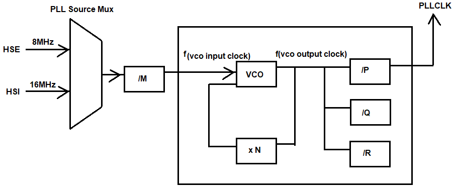
So looking at this diagram, the source of the PLL clock can either be the HSI or HSE clock signal.
There is then a divider labeled /M.
This allows us to divide the frequency into a value less than the HSI or HSE signal.
It is important to know that the frequency of the vco input clock signal must be between 1-2MHz.
Therefore, if we are using the 16MHz HSI clock signal, then you can divide it by either 16 or by 8.
The multiplier is labeled x N.
We can specify any value to this multiplier up until its limit.
For example, if we want 50MHz, you can set x N to 100 to get a 100MHz clock signal.
This then would make the /P divider 2, to turn the 100MHz to 50MHz.
The /P divider must be at least a value of 2. It can be given a value of either 2, 4, 6 or 8.
The /P divider is the final component that determines the value of the PLLCLK. The output frequency after the /P divider cannot exceed 180MHz.
The /Q and /R dividers are for specific peripheral devices and, thus, we do not change them from their original default values. By default, they are equal to 2. We do not need to modify them. According to the datasheet, PLLQ is the division factor used for USB OTG FS and SDIOclocks. PLLR is the division factor used for I2Ss, SAIs, SYSTEM and SPDIF-Rx clocks.
All of this can be used in the datasheet below in the
RCC PLL configuration register (RCC_PLLCFGR).
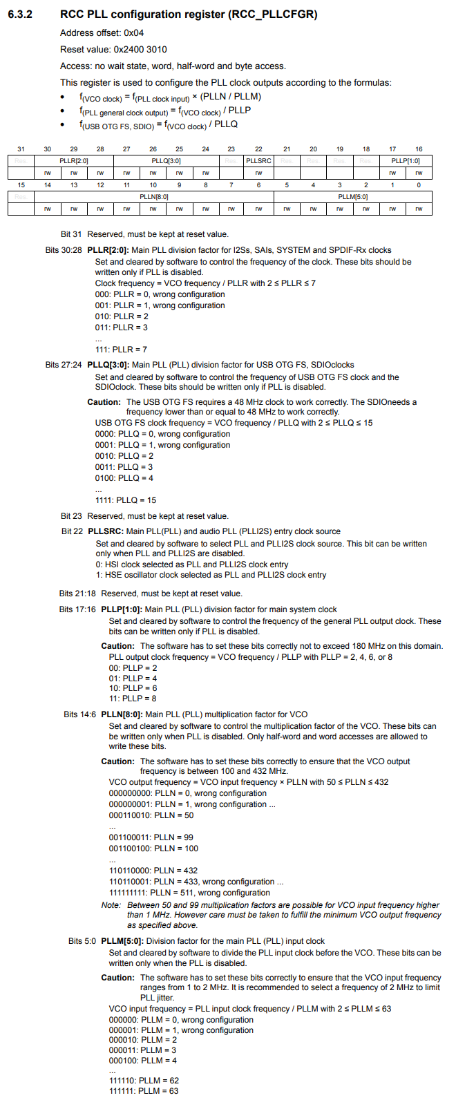
You can see that this register has bits reserved for PLLM, PLLN, PLLP, PLLQ, and PLLR in order for us to select the necessary clock configurations.
The nucleo STM32F446 board has a maximum frequency of 180MHz for the SYSCLK signal. So this value cannot be exceeded for the PLLCLK output. You must also respect the frequency constraints for each of the peripheral buses, including the APB1 bus and the APB2 bus. The APB1 bus can have a maximum frequency of 45MHz and the APB2 bus can have a maximum frequency of 90MHz. These we will set too in our program.
This code goes within the main.c file within the Core directory.
We will now go through the code.
We must include the necessary files, including the main.h file, which includes the definitions of the sys clock frequencies. It is common to include definitions used in the main.c in the main.h header file, if they aren't already included in other files.
We have our main() function, which calls the HAL_Init() function, which is used to initialize various clock settings.
We then have the line, SystemClock_Config(SYS_CLOCK_FREQ_50_MHZ);SystemClock_Config(SYS_CLOCK_FREQ_50_MHZ);
This allows for the initialization and setup of the PLL clock that will output 50MHz.
We use switch statements to create 3 possible PLL clock outputs: 50MHz, 84MHz, and 120MHz.
We now go over the SystemClock_Config() function.
The osc_init and clk_init are 2 handlers, which will initialize the PLL clock (in the case of osc_init) and the peripheral clock buses (in the case of clk_init).
The FLatency corresponds to the flash latency. This deals with the relation between CPU clock frequency and flash memory read time. To correctly read data from Flash memory, the number of wait states (Latency) must be correctly programmed in the Flash acccess control register (FLASH_ACR) according ot the frequency of the CPU clock (HCLK) and the supply voltage of the device.
We initially set FLatency to 0, but when defining each of the cases for the different frequency system clocks, we set it to the appropriate number of wait states based on the frequency in use.
For 50MHz, 1 WS (2 CPU cycles) are needed in order for data to be read correctly from Flash memory.
For 84MHz, 2 WS (3 CPU cycles) are needed.
For 120MHz, 3 WS (4 CPU cycles) are needed.
This can be seen in the datasheet section 3.4, which is shown at the following link: Flash Latency- Nmber of Wait States According to CPU Clock (HCLK) Frequency in an STM32F446 Board
We then initialize the osc_init settings.
The OscillatorType is HSI because our clock source is an HSI clock source which is fed into the PLL engine to produce an output signal.
Next, we turn on the HSI clock through the HSIState attribute.
We set the HSI clock frequency to the default frequency of 16MHz through the HSICalibrationValue attribute. \
So we then create a switch statement in which we have various cases of diffrent clock frequencies.
We then turn on the PLL clock through the PLL.PLLState attribute.
We set the source of the PLL clock to be from the HSI clock signal.
We then set the PLL dividers and multiplier, which determin the frequency of the output signal.
Being that we set the HSI signal to be 16MHz, we then divide it by 16 through /M to get a 1MHz signal. We then multiply this value by 100 through x N to get 100MHz. We then divide this by 2 through /P to get an output clock signal of 50MHz.
We set the SYSCLK source to be the PLLCLK.
We set the AHB prescaler to /1, which keeps the signal at the same frequency.
We set the APB1 prescaler to /2, which sets the signal to 25MHz.
We set the APB2 prescaler to /2, which sets the signal to 25MHz.
Because the frequency of the clock is 50MHz, the flash latency must be set to 1 WS.
We then use a break statement to end this case of a 50MHz PLL clock signal.
We then go to the case of a 84MHz clock signal.
For this, we again divide the signal by 16 to get 1MHz. We then multiply this signal by 168 to get 168MHz, which we divide by 2 to get 84MHz. We set AHB to be 84MHz, and APB1 and APB2 to be 42MHz.
For 84MHz, the flash latency needs to be 2 WS.
We then use a break statement to end this case of a 84Mhz PLL clock signal.
We then go to the case of a 120MHz clock signal.
For this, we again divide the signal by 16 to get 1MHz. We then multiply this signal by 240 to get 240MHz, when we divide by 2 to get 120Mhz. We set AHB to be 120MHz, APB1 to be 30MHz, and APB2 to be 60MHz.
Remember that APB1 can have a maximum frequency of 45MHz, while APB2 can have a maximum frequency of 90MHz. So this must be taken into account when assigning clock frequencies to buses of the microcontroller board.
Since the frequency is 120MHz, we need a flash latency of 3 WS.
We then have a break statement to end this case.
We do not have a default case, so we simply have a return statement.
We then have 2 if statements to handle errors.
We then do systick configuration.
The only other thing that's important to be done is the main.h file, which will have definitions for the 3 cases of the 3 different clock frequencies.
Add the following lines to the main.h file.
So after this, the program should run without any
errors and you can specify either a 50MHz, 84MHz, or 120MHz PLL clock signal
as output.
And this is how to configure a PLL clock from an HSI clock source
in an STM32F446 board.
Related Resources