
How to Enable the Peripheral Clock of the STM32407G Microcontroller Board in C
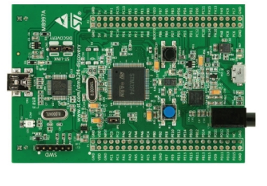
In this article, we show how to enable the peripheral clock of the STM32F407G microcontroller discovery board in C.
Enabling the peripheral clock is very important because in order to use any peripheral device, whether it be the ADC or any timer or SPI communication or UART communication, the peripheral clock for that device must be enabled.
Without the peripheral clock being enabled for a peripheral component, the component essentially cannot be used.
In order to enable the peripheral clock for a device, one of the most vital things that you must know is the bus that the peripheral device is connected to.
From this bus, you can then turn on the peripheral device for a component connected to that bus.
So, for example, let's create the C code that will turn on the peripheral clock for the ADC1 component, which is one of the ADC components on the microcontroller board.
So you can know which bus a peripheral device is connected to through 2 main different means.
One way is you can look at the memory map of the microcontroller board.
Below is one section of the memory of the STM32F407G microcontroller board.
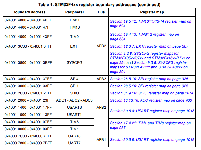
So in the memory map, you can see there's a column called bus, which tells you which bus the peripheral device is connected. For all the ADC components, you can see that they are all connected to the APB2 bus. So this is the bus that we need to configure when we are enabling the peripheral device.
Another way you can tell which bus a peripheral device is connected to is by looking at the block diagram of the microcontroller.
The block diagram for the STM32F407G microcontroller board is shown below.
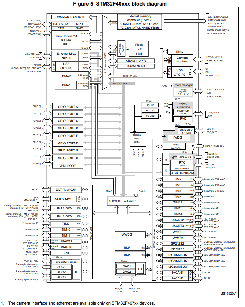
You can see at the bottom left the ADC devices and how they are connected to the APB2 bus.
So now we know the bus that the ADC peripheral devices are connected to .
This is the first step in turning on the peripheral clock- you must know the bus the peripheral device is connected to.
Now you must know that the microcontroller board has a base clock which works off of the base address, 0x4002 3800
Every peripheral clock on any of the other buses works off of this base address with its assigned address offset. This base address with the address offset is the address for the specific bus.
In order to turn on a peripheral device, we need to go the clock enable register for the bus that the peripheral component is connected to, and enable the peripheral clock for that device.
So the ADC components are connected to the APB2 bus, so we need to go to the RCC APB2 peripheral clock enable register (RCC-APB2ENR).
This is shown below.
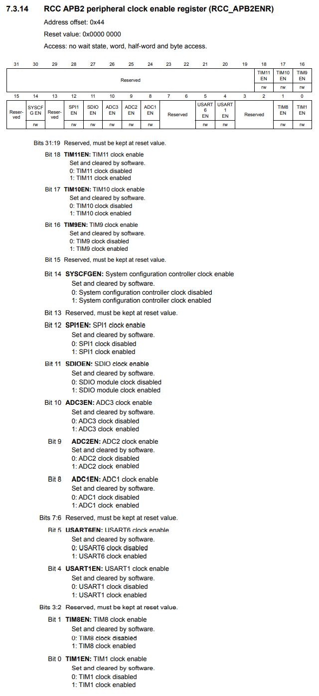
Each bus has its own clock enable register, with all the components connected to it represented in its bits.
If you want to turn on the peripheral clock for the ADC1 component, then you would set bit 8 to HIGH (1).
So this is how we can enable the peripheral clock for a peripheral component.
Below is the complete code for enabling the peripheral clock for the
ADC1 component in an STM32F407G microcontroller board.
So let's now go over the code.
So we need to be able to address the APB2 bus, which is the bus the ADC component is connected to it.
To do this, we first need the base address of the RCC register, which is 0x4002 3800
We then need the offset to get the APB2 bus address. The offset is 0x44
By the way, UL stands for unsigned long
We then get the total address by adding the base address with the offset address.
We then have our main function.
We create a 32-int pointer variable which points to the full address of the APB2 register.
We then set pin 8 HIGH, which turns on the peripheral clock for the ADC1 device.
Now this code doesn't do anything that we can visually on the STM32FG407G microcontroller board, but we may want to know if what we wrote is actually occurring.
For this, we can go to the Window Tab and go down to Show View and click on SFRs.
Within SFRs, we click on RCC, then click on APB2ENR register.
You should then see the ADC1EN bit.
After stepping through the code, this bit should have a value of 0x1, which means that the peripheral clock is enabled for the ADC1 device.
This is shown in the image below.
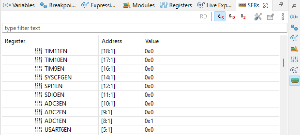
So we can see that our code has achieved the objective of turning on the
peripheral clock for the peripheral we wanted, in this case, ADC1.
So this is how to enable the peripheral clock for a peripheral device
in an STM32F407G microcontroller board in C.
Related Resources