
How to Output a Clock Signal from a Microcontroller Clock Output (MCO) Pin with a STM32F407G Discovery Board in C
In this article, we go over how to output a clock signal from a microcontroller clock output (MCO) pin with an STM32F407G discovery board in C.
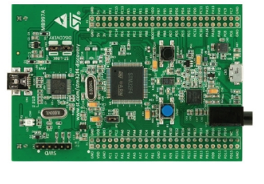
The STM32F407G discovery board has 2 microcontroller clock output (MCO) pins.
These are the pins, MCO1 and MCO2.
The MCO1 pin can output a clock signal either from HSI (high-speed internal clock), LSE (low-speed external clock), HSE (high-speed external clock), or a PLL (phase locked loop).
The MCO2 pin can output a clock signal either from the HSE clock, PLL clock, system clock (SYSCLK), or PLLI2S clock.
In this article, we are going to output a HSI clock signal from the MCO1 pin.
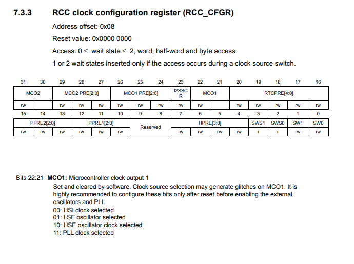
The HSI clock signal, again, is from the internal clock system. This is configured with the RCC clock configuration register (RCC_CFGR).
It is important to note that, again, the MCO1 pin is PA8, which is pin 8 of GPIO PORTA. In order for this pin to function as MC01, it needs to be set in alternate function mode.
Alternate function mode allows pins such as GPIO pins which can function as general purpose I/O pins to have alternate functions, such as in the case of pin PA8 to be a MCO pin.
Once this pin is set in alternate function mode, we can output a clock pin through it. This clock pin can then be measured through a device such as an oscilloscope or logic analyzer.
Our program does not utilize any prescalers, so it outputs the 16MHz signal that the HSI clock emits originally without a programmer applying any modifications.
There are a number of steps that need to be done to make this clock output signal occur.
First, we must configure the RCC Clock Configuration Register to select the HSI clock to be output from the MCO1 pin.
Then we must enable and turn on the clock for the peripheral register GPIO PORTA, since we are outputting the clock signal from pin PA8.
Then we must configure pin PA8 to be in alternate function mode, so that it can act as a MCO pin.
We then set pin PA8 to mode 0 in the alternate function high register.
At the end of this, we should be able to read and measure a 16MHz signal from pin 8 of GPIO PORTA.
Before we explain the code, let us just look first at the clock-out capability of the MC0 pins.
This is shown below in the clock-out capability of the MCO pins in the datasheet, which you can find at the following
link: STM32F4xx Datasheet.
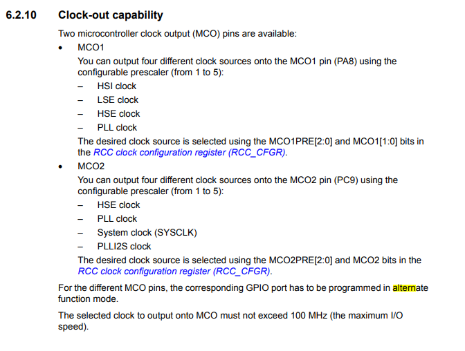
We can see that for this MCO pin, MC01, that we are working with, we can output a clock signal from HSI, LSE, HSE, and PLL clock signals.
In this case, we will be doing so with an HSI clock signal, which is internal to the microcontroller.
We now will explain the code.
At the top of our code, we include the Next, we have several macros defined which define the addresses of memory mapped devices such as clocks
and general purpose I/O ports (PORTA in this case). We will go over these more.
So within our main function, we first define the RCC Clock Configuration Register (RCC_CFGR).
This register allows us to select the type of clock we want to use for the microcontroller and where we want to output the signal
from.
So looking at the RCC clock configuration register above, in order to output a
HSI signal from the MCO1 pin, we need to set bits 21 and 22 to 00. This is how we can get the HSI signal
to output from pin 8 of GPIO PORTA, which is MC01 when the pin is in alternate function mode.
So the first thing you have to do with any register is to assign it an address, so that
the program knows which register you are referencing.
The address of the RCC clock configuration register is the base address of the RCC
clock register plus the offset of the RCC clock configuration register, which is 0x08
We then clear bits 21 and 22 in order to output a HSI clock signal from the MCO1 pin.
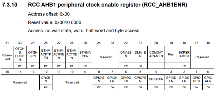
Next we must enable and turn on the peripheral clock for the GPIO PORTA register. This is
the register that contains the MCO1 pin, which is pin 8.
In order to enable the peripheral clock for GPIO PORTA, we use the base address of the
GPIO PORTA register plus the offset of the RCC AHB1 bus; this is the bus that is connected to GPIO PORTA.
When enabling peripheral registers, you get the base address of that address plus the offset
of the bus it is connected to.
Below is the RCC AHB1 peripheral clock enable register.
Looking at the RCC AHB1 peripheral clock register, we see that this register has an
address offset of 0x30. What this means is that we have to add the base address of RCC to this address offset of
0x30. This gives us a result of, 0x4002 3800 + 0x30
This address gives us the address for the RCC AHB1 peripheral clock register, which is the
register that allows us to work with the GPIOA and GPIOD ports.
A bus, such as the AHB1 bus, is connected to multiple registers, such as other GPIO ports,
clocks, and memory devices. In the code, you then have to configure it to turn on the specific register
that you want, in this case, GPIO PORTA. You can see based on the diagram that setting the 0th bit to
1 enables the peripheral clock for the GPIO PORTA.
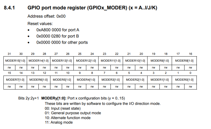
The next thing we need to do is use the GPIO port mode register to set pin 8 in alternate
function mode. This will allow it to act as a MCO pin, MC01, specifically.
This register has no offset, so it's the same address as the base register for the
GPIO PORTA register.
Below is the diagram for the GPIO port mode register.
You can see that bits 16 and 17 control the mode of pin 8.
Setting these bits to 10 in binary or 0x02 in hexadecimal sets this pin to alternate
function mode.
We first clear the bits with the line, *pGPIOAModeReg &= ~(0x3 << 16);
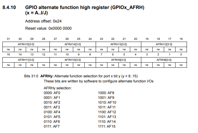
The last thing we need to do is set the mode of the GPIO Alternate Function High Register
to mode 0, which sets pin 8 to mode 0.
The diagram for this register is shown below.
Again, we set up the addresses appropriately to reference this register and then we clear the first 4 bits of the
register to set pin 8 to mode 0.
After this, we loop the code forever.
Now we should be able to get a 16MHz clock signal from pin 8 of the GPIO PORTA.
If you take a measuring device such as an oscilloscope or logic analyzer that has a maximum frequency reading above 16MHz,
you should be able to read this 16MHz square wave signal from this pin.
You do this by placing the positive probe to pin 8 and the negative probe to ground on the microcontroller board.
And this is how to output a clock signal on a microcontroller clock (MCO) pin with a STM32F407G discovery board
in C.
Related Resources
How to Set Bits of a Number in C
How to Clear Bits of a Number in C