
How to Transmit Data with the SPI Communication Protocol with an STM32F407G Microcontroller Board in C
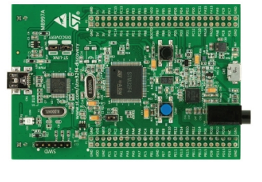
In this article, we explain how to transmit data with the SPI communication protocol with an STM32F407G microcontroller board in C.
SPI stands for serial peripheral interface, and it is often used to transmit data between components on a microcontroller board.
SPI is best used for short distances and covers a distance of less than 10 feet.
It is a high-speed communication protocol that has no maximum clocking time.
SPI communication uses 4 pins: SCLK, MOSI, MISO, and NSS.
In full duplex mode, 4 pins need to be connected from the master device to the slave device.
However, in other simpler configurations, such as half duplex mode where there is only transmission from the master to the slave without any reception of data from the master, 2 pin connections can be sufficient.
In this simple configuration, the SPI connection needs only a clock and a MOSI connection.
This is what we will do in our circuit.
We don't need configure or do anything with the MISO pin and the NSS pin in terms of physical connections.
In fact, in this project, we won't be connecting any two devices together for SPI communication.
Instead, we simply show how to transmit data from the MOSI pin.
We can then use a logic analyzer to detect whether this data was sent correctly from this MOSI pin.
So, in this project, let's do this.
We use SPI1 for our SPI communication.
SPI can be used by setting alternate functionality to specific pins on the GPIO Port A register.
Below is the diagram of the alternate function mapping
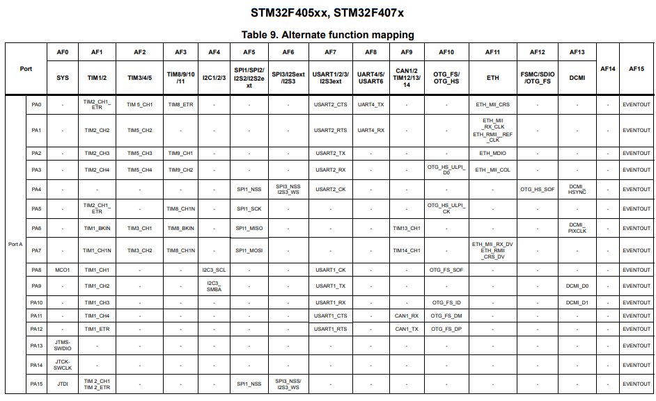
You can see that if we configure the GPIO Port A pin 4 in AF5, it now functions as SPI1_NSS.
If we configure PA5 in AF5, it now functions as SPI1_SCK (the clock).
If we configure PA6 in AF5, it now function as SPI1_MISO.
If we configure PA7 in AF5, it now function as SPI1_MOSI.
Once these configurations are made, these pins function as the SPI connections to the outside world (or the slave device, if there is a slave connected).
If our case, we simply leave these pins configured but unconnected and then use a logic analyzer to analyze the SCK signal and the contents transmitted through the MISO pin.
We need 2 major code files in order for this code to work.
We need our header file, which contains many macros and structures that describe the various registers and needed values.
We then need our main C file, which contains the code that allows us to send the text, "Hello World" out from the MOSI pin of the STM32 board, along with an 8MHz clock signal on the SCK pin.
Below is the header file that we will need for our code, which in this case is named,
stm32f407xx.h
So this header file contains all the definitions we need to create our main C file.
The contents of the main.c file is shown below.
The first thing we must do is include the string header file and our stm32f407xx.h header file in our main.c file.
We next have our main function.
So when dealing with a board like the STM32 board, sending a string through SPI communication is sending a character one at a time through transmission.
Remember that SPI is serial communication. So only one byte is sent at a time when the data frame format (DFF) is 8 bits. Remember that an ASCII character is a byte, or 8 bits. Therefore, only one character is sent per clock cycle.
So we declare the data type to be an array of characters and we set this equal to, "Hello world"
Next we need to turn on the appriopriate clocks for the periphery. This includes the GPIO Port A and SPI1.
Next we set all of the GPIO Port A pins needed for SPI1. This includes pins 4, 5, 6, and 7. Even though we don't use all of them, we configure them.
We use the MODER register to set all of these pins in alternate functionality mode.
After putting them all in alternate functionality mode, we have to set the AFRL to AF5, which allows them to act as pins for SPI1. This is all done in the AFRL register because all of the pins are from pins 0 to 7.
Pin PA4 will act as SPI1_NSS
Pin PA5 will act as SPI1_SCK
Pin PA6 will act as SPI1_MISO
Pin PA7 will act as SPI1_MOSI
Now we do some configurations directly in the SPI control register 1.
The SPI control register 1 is shown below.
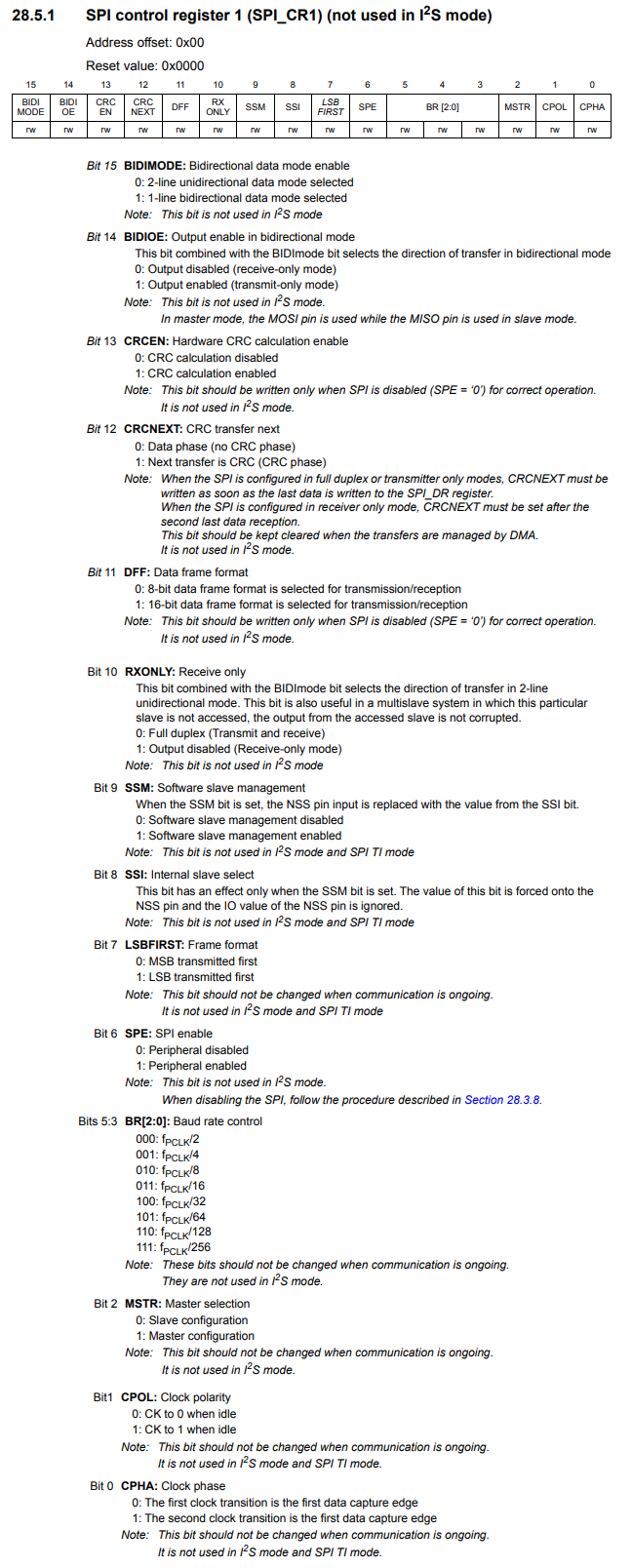
With this register, we can configure the SPI communication for full duplex mode. This is the default, so we do not need to make any configuration changes.
The first thing we do is set the STM32 board as the master device. This is done by writing a HIGH value to bit 2, the MSTR bit.
The master device is the entire STM32 board.
The STM32 board transmits data which can then be received by a slave device.
A slave device or multiple slave devices can then send data to the STM32 board (if slaves are connected).
We keep the default setting of the clock which is FPCLK/2. Since the internal RC oscillator clocks has a frequency of 16MHz, the SCK for SPI communication will be 8MHz.
Next, since we do not need to use the NSS pin in this project, since we are not connecting a slave device, we should disable it. We can disable it in software by setting the SSM bit, bit 9, to 1. This enables software slave management.
We then have to set SSI, bit 8, to 1. This forces the SSI bit HIGH. We disable the NSS pin of the master device by connecting it to VDD. NSS cannot be connected to ground because if it is, it will trigger a MODF error, and our program won't run. If NSS is to be unused, it should be connected to HIGH voltage.
Lastly, we must enable the SPI for communication by setting the SPI enable bit, bit 6.
We do this last because as soon as this is enable, the SPI begins communication, so all configurations of the SPI communication must be done before this.
Next, we need to know how many bytes of data we are transmitting. We store this in the len variable. We do this in order to use a while loop so that the STM32 board will keep sending bytes until there are no more.
Next we create an 8-bit pointer variable, *pTxBuffer, which we set equal to user_data.
We then have our while loop that will execute as long as there are still bytes to transmit.
Before we transmit any bits, we want to make sure that the transmit buffer, bit TXE, bit 1, in the SPI status register is empty.
The SPI status register is shown below.
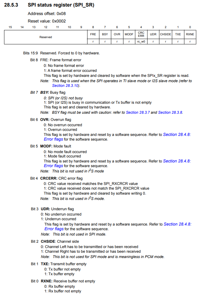
The status register is a register composed of various flags and status buffers that lets us know the status of various things.
When transmitting data, we want to know that the transmit buffer is empty. Once it is empty, we can then write to the data register, which will then overwrite contents in the transmit buffer.
We wait for the transmit buffer to be empty through the line, while(!(pSPI1->SR & (1 << 1)));
The SPI data register is shown below.
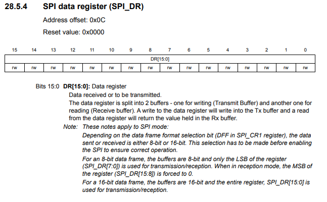
The data register is 16 bits in size.
Next, we write 2 generic cases, where we are transmitting data in a data frame format of 16 bits and the other with 8 bits.
If the DFF is 16 bits, we write the 16 bits to the data register. Because we are transmitting 16 bits, or 2 bytes, we decrease the len variable by 2.
We then increment the pointer by 2, so that we can write the next 16 bits to the data register in the next transmission.
If the DFF is 8 bits, we write 8 bits to the data register. Because we transmit only one byte, we decrease the len variable by 1. We increase the pointer by 1, so that we can write the next 8 bits to the data register.
Once the while loop is exited, we just want to do one final check to make sure the SPI communication protocol is finished with all processing.
We want to check the busy flag in the SPI status register to make sure that is not busy.
Therefore, we add the 7th bit with a 1.
If the busy flag is 1, it will remain in the while loop until it is changed to 0, in which it exists the while loop.
We then disable SPI1 by clearing the SPE bit, bit 6, of the SPI control register 1.
So this is our program.
We can now use a logic analyzer and a good software program to analyze the SCK pin, which is pin PA6, and the MOSI pin, which is pin PA7.
You do this by placing the positive probe on each of these pins and the negative probe to ground.
With a good analysis software, you can see the text transferred through the MOSI pin.
So this is how to transmit data with the SPI communication protocol with an STM32F407G microcontroller
board.
Related Resources