
How to Build a Keypad Circuit with a STM32F407G Discovery Board in C
In this article, we go over how to build a keypad circuit with an STM32F407G discovery board in C.
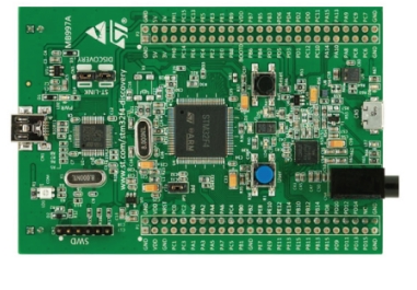
We show how to connect a keypad to a STM32F407G discovery board so that we can press keys and have our software process these key presses.
The keypad we will use in this article is a 4x4 keypad.
This is shown below.
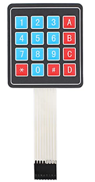
This keypad has 16 keys, 1,2,3,4,5,6,7,8,9,0,A,B,C,D,*,#.
This keypad has 8 pins that allow electrical connection to the STM32F407G discovery board.
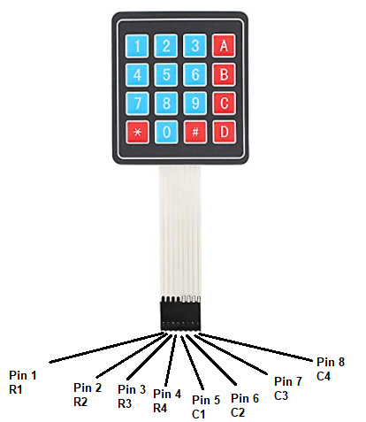
How the keypad works is an electrical grid of rows and columns.
As you can see above, the keypad has 4 rows and 4 columns.
The first 4 pins of the keypad, looking at it from left to right, are the row pins, R1, R2, R3, R4.
The next 4 pins of the keypad are the column pins, C1, C2, C3, C4.
This is shown in the pinout diagram below.
By connecting these pins to GPIO pins on a port of the board, we can then use software to monitor if a key has been pressed or not and which one by examining the logic status of each row pin and each column pin.
The full schematic to build the circuit is shown below.
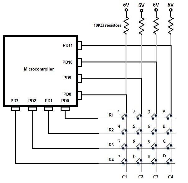
So we utilize PORTD pins to attach the pins of the keypad to.
We attach the 4 row pins to pins PD0, PD1, PD2, and PD3.
We attach the 4 column pins to pins PD8, PD9, PD10, and PD11.
Even though you see pull-up resistor attached to each of the columns, you don't have to do this connection physically. This is because we can simulate internal pull-up resistors in software, which is what we do in our code. This makes for less hardware.
Also there is no need for hardware compensation for button debouncing because we will do this in software by adding in delays into our program.
So let us now get into our program.
We now will explain the code.
We first create a delay function, which we will use later in our code in order to add a delay in order to counter button debouncing.
Button debouncing is a phenomenon that occurs when a user presses down a button, which creates an electrical connection with each button press. Normally what is intended is that the button will pressed once. However, in order to prevent the key press from being registered multiple times within a very short period of time, we must add a certain delay so that only one press occurs within that time frame, usually a few milliseconds, such as 200ms or so (1/5 of a second). Otherwise, we won't get a smooth user experience with our keypad.
Next, we define our peripheral registers.
These are the registers we must use during our program in order to have a functioning keypad.
The first register is GPIO port D register, represented by the variable, pGPIODModeReg
If you look this up in the memory map of the datasheet for the STM32F407G discovery board, this port has a base memory address of, 0x40020C00
In order to make certain pins of GPIO port D input pins, we need to access the GPIO port input data register. This uses the GPIO port D as the base address with an added address offset of, 0x10
In order to make certain pins of GPIO port D output pins, we need to access the GPIO port output data register. This uses the GPIO PORT D as the base address with an added address offset of, 0x14
We then need to enable the peripheral clock register for the GPIOD port. The RCC, the Reset and Clock Control, for the board handles clock control. According to the memory map, the base address for the RCC is, 0x4002 3800 So RCC forms the basis for all clock control and above is the base address for RCC. What we want to do is enable the peripheral clock register, specifically for GPIOD. We enable the peripheral clock reigster via the RCC AHB1 peripheral clock register. Looking at the RCC AHB1 peripheral clock register, we see that this register has an address offset of 0x30. What this means is that we have to add the base address of RCC to this address offset of 0x30. This address gives us the address for the RCC AHB1 peripheral clock register, which is the register that allows us to work with the GPIOD port.
Next, since we want to avoid the hassle of connecting pull-up resistors physically to each of the column connections, we do this in software. Yes, you're capable of doing this in software rather than hardware. We can enable pull-up or pull-down resistors by the GPIO port pull-up/pull-down register. You use the GPIO port D base address with an offset of 0x0C. This references the GPIO port pull-up/pull-down register. As with all registers in the STM32F407G discovery board, this is a 32-bit register that references each of the 15 I/O pins of a port. Each pin is referenced by 2 bits. To specify a bit be used as a pull-up resistor, you would specify 01 for that pin in this register.
To enable the clock register specifically to work with GPIOD. we must set bit 3 (4th bit) of the RCC AHB1 peripheral clock register to a HIGH value.
Next, we need to set pins PD0, PD1, PD2, and PD3 as output pins. This is simply because this is how to configure a keypad to a software application. So we want to set these 4 pins, again, PD0, PD1, PD2, and PD3 as output pins.
The *pGPIODModeReg allows us to select which pins will be inputs and which will be outputs.
Again, like all registers, te GPIO port mode register is a 32-bit register, which allows us to select which pins will be inputs and which will be outputs. Each of the 15 pins can be referenced by 2 bits.
A 00 represents the pin is an input.
A 01 represents the pin is an output.
Since we want pins, PD0, PD1, PD2, and PD3 to be outputs, this represents 01 01 01 01. Because each hex digit is represent by 4 bits of binary digits, the hex equivalent is 0x55.
Before we do this, it's a good habit to clear all the bits throughout the entire register, just so that everything is clear, started out on a fresh slate. We do this through the line, *pGPIODModeReg &= ~(0xFF); We then set pins PD0, PD1, PD2, and PD3 as outputs by the line, *pGPIODModeReg |= 0x55;
After setting the row pins as outputs, we then have to set the column pins as inputs. We do through the same GPIO port mode register. The column pins are connected to pins, PD8, PD9, PD10, and PD11. So this is done through clearing all the bits from PD8 to PD11. PD8 starts at bit 16. So we need to clear 8 bits starting from bit 16 to make PD8 to PD11 input pins. This is done through the line, *pGPIODModeReg &= ~(0xFF << 16);
Next, we have our while function.
This is the code that executes over and over in an infinite loop.
This first thing we have to do is make all rows HIGH. This is the equivalent to initializing the rows to an unselected state. This is done through the line, *pOutputDataReg |= 0x0f;
We then make R1 (PD0) LOW. This is the equivalent to R1 being selected. This is done through the line, *pOutputDataReg &= ~(1 << 0);
The next thing we need to is scan the columns to see which column is selected. Remember that all columns are active HIGH via the pull-up resistors we created in code. What we want to do is check to see if any goes LOW, meaning it's pressed.
The variable, *pInputDataReg, is the register that contains the data of the input pins of the PORTD register. By ANDing this with (1 << 8), we check the 8th bit. Remember that the input pins are normally HIGH via the pull-up resistors. So if the input pin is HIGH, and it is ANDed with a 1, it will produce a 1 which will then be negated by the ! (NOT) symbol and produce 0. Therefore, the character will not be printed. However, if the key is pressed, the variable, *pInputDataReg, will be LOW or 0. A 0 ANDed with 1 is 0. With the ! (NOT) symbol, this produces a 1, and the character will be output.
After each scan, we add a delay, because of button debouncing. We account for this in software with the delay() function. This will ensure that the key press won't trigger multiple repetitive keys with a quick momentary press. A certain period of time must pass before the key is repeated with a press. Triggering multiple keys with a quick momentary press would create a bad user experience.
So with R1 LOW, we check this for PD8, PD9, PD10, and PD11.
If R1 is LOW and PD8 is LOW, a '1' is output.
If R1 is LOW and PD9 is LOW, a '2' is output.
If R1 is LOW and PD10 is LOW, a '3' is output.
If R1 is LOW and PD11 is LOW, an 'A' is output.
We then set all rows HIGH to reset all rows to an unselected state.
We then set R2 LOW.
If R2 is LOW and PD8 is LOW, a '4' is output.
If R2 is LOW and PD9 is LOW, a '5' is output.
If R2 is LOW and PD10 is LOW, a '6' is output.
If R2 is LOW and PD11 is LOW, an 'B' is output.
We then set R3 LOW.
If R3 is LOW and PD8 is LOW, a '7' is output.
If R3 is LOW and PD9 is LOW, a '8' is output.
If R3 is LOW and PD10 is LOW, a '9' is output.
If R3 is LOW and PD11 is LOW, an 'C' is output.
We then set R4 LOW.
If R4 is LOW and PD8 is LOW, a '*' is output.
If R4 is LOW and PD9 is LOW, a '0' is output.
If R4 is LOW and PD10 is LOW, a '#' is output.
If R4 is LOW and PD11 is LOW, an 'D' is output.
This is how we are able to check which key is pressed with a keypad connected to an STM32F407 discovery board.
And this is how to build a keypad circuit with a STM32F407G discovery board
in C.
Related Resources
How to Set Bits of a Number in C
How to Clear Bits of a Number in C