
How to Build a Logic Probe
In this project, we are going to build a logic probe using a 4011 NAND gate chip.
This logic probe will light up green if the logic signal is HIGH and red if the logic signal is LOW.
So it works pretty much like a typical logic probe.
This logic probe will be built using a single chip, the 4011 NAND gate chip.
This chip consists of 4 NAND gates, and being that it's composed of NAND gates, it works very well with logic inputs. So it's great for building a logic probe, since it's composed of logic gates.
In this project, we will use 3 out of the 4 NAND gates. Using 3 out of the 4 is sufficient for building a logic probe.
Below it will be explained in depth how to wire up the 4011
NAND gate chip so that
it can function as a logic probe.
Components Needed
- 4011 NAND Gate Chip
- Green LED
- Red LED
- 2 470Ω resistors
- Power Source
The pinout of the 4011 is shown below, so that you can see how to connect it in the circuit.
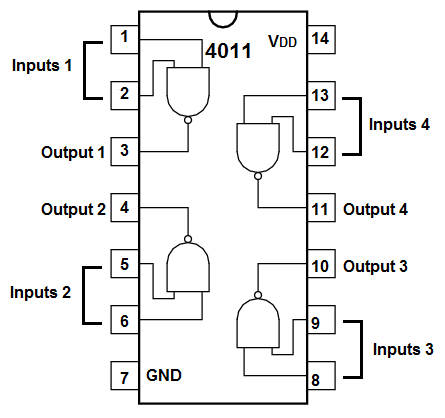
Each NAND gate has input pins and 1 output pin.
The following chart shows NAND gate logic, which shows what output a NAND gate chip will produce for a set of given inputs.
| NAND Gate Logic | ||
| Inputs | Output | |
| 0 | 0 | 1 |
| 0 | 1 | 1 |
| 1 | 0 | 1 |
| 1 | 1 | 0 |
This chart serves as the reference for NAND gate logic. You will use as a reference to know what output state the NAND gate will produce for a given set of inputs.
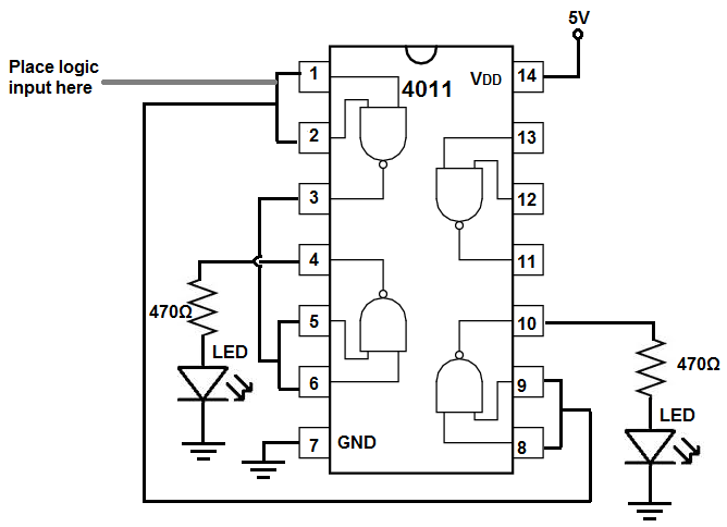
How this circuit will work is the first 2 NAND gates will be converted into an AND gate. The 2 inputs will be tied together, so that they're common. So if the logic input is a HIGH, it will produce 2 HIGHs as the logic inputs. When there are 2 HIGH inputs into a logic gate, this will produce a HIGH at the output. Therefore, the LED will turn on. This is the case for the AND gate (converted from AND gates).
We will use a third NAND gate which will be unconverted. We will use it purely as
a NAND gate, as it is. The 2 inputs into the NAND will be tied together, common. Then the input will
be tied in with the input from the AND gate. Therefore, we can get dual functionality, so to speak.
The circuit can now light up green when there is a logic level of 1 and light up red when there is a logic level
of 0.
Logic Probe Circuit
The logic probe circuit we will build to read logic levels is shown below.
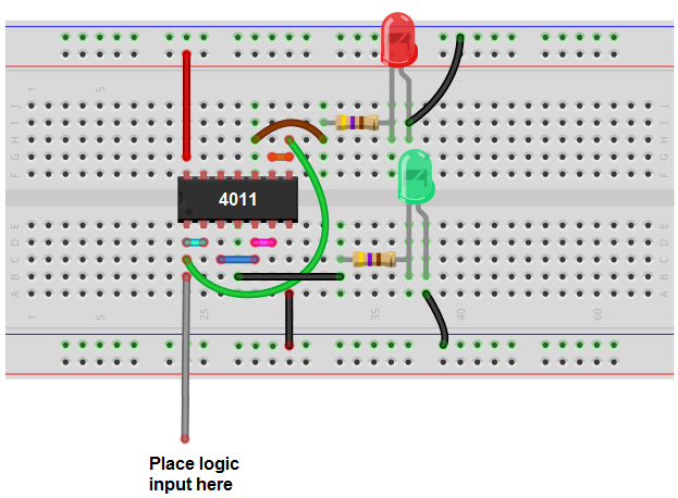
This above circuit built on a breadboard is shown below.
This logic probe will light up the green LED when the logic input is HIGH (a 1) and will light up the red LED when the logic input is LOW (a 0).
Again, how this works is that the first gate, which uses 2 NANDs, is converted into an AND gate. An AND gate will only produce a HIGH on the output when both inputs are HIGH. So the output of the AND gate contains the green LED. When the logic input is HIGH, then the green LED will turn on, indicating a logic HIGH has been detected.
Now the next gate is a pure NAND gate (unconverted). NAND gates give a HIGH at the output when either input is LOW. So when there is a logic LOW input, then the NAND gate will produce a HIGH at the output, which will turn on the red LED.
And this is how a simple logic probe works. And there are many variations we can do of this circuit. Instead of lighting up LEDs, we can make it so that a buzzer sounds. It all depends on your preference. In this case, the circuit would actually be simplified. If we have a logic probe that beeps only when there is a logic HIGH input, then all we would need is the AND gate and we wouldn't a third gate. So build the circuit to suit your preferences.
This logic probe circuit is a very simple and lacks the sophistication of most commercial ones which can detect pulses (signals that change between high and low repeatedly).
Related Resources
How to Build a Dark-activated Switch