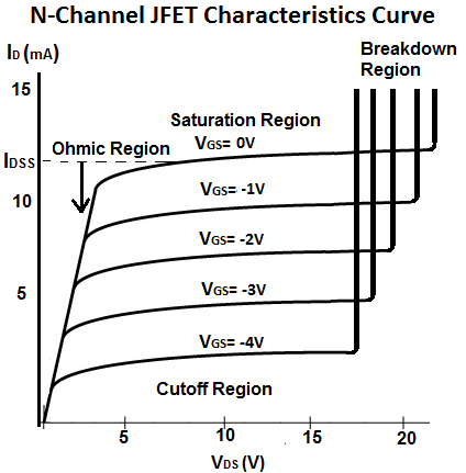
N-Channel JFET Characteristics Curve
The transconductance characteristics curve of a JFET transistor is the the curve which shows the graph of the drain current, ID verses the gate-source voltage, VGS.
The ratio of change in drain current, ∆ID, to the change in gate-source voltage, ∆VGS, is the transconductance, gm. This is what this characteristic curve serves to show.
The transconductance curve, as for all semiconductor devices, is nonlinear, for most of the curve, meaning changes to VGS do not directly increase or decrease drain current, ID.
Below is the characteristic curve for an N-Channel JFET transistor:
How an N-Channel JFET Works
An N-Channel JFET turns on by taking a positive voltage to the drain terminal of the transistor and a gate-source voltage, VGS, between 0V and -4V. It shuts off by taking in a negative gate-source voltage, VGS, below -4V.
You can see based on this N channel JFET transconductance curve that as the negative voltage to the gate increases, the gain decreases. You can see that the gain, the current ID output by the transistor, is highest when the voltage fed to the gate terminal is 0V. As we increase this voltage (negatively), again, as stated, the gain decreases.
This transconductance curve is important because it shows the operation of a N channel JFET.
You can also see that the transconductance curve, as for all semiconductor devices, is nonlinear, for most of the curve, meaning changes to VGS do not directly (linearly) increase or decrease drain current, ID, even though this is a lesser issue.
The big point is that, an N-Channel JFET turns on by having a positive voltage applied to the drain terminal of the transistor and ideally no voltage applied to the gate terminal. The transistor circuit shuts off by taking in a negative gate voltage, VGS, greater than about -4V or so. The transistor is in its fully conductive state and is in maximum operation when the voltage at the gate terminal is 0V. As we increase the amount of negative voltage the gate terminal receives, the transistor becomes less conductive. Once the negative voltage reaches a certain threshold, the N channel JFET circuit stops conducting altogether across the drain-source terminal.
The Regions that make up a transconductance curve are the following:
Cutoff Region- This is the region where the JFET transistor is off, meaning no drain current, I D flows from drain to source.
Ohmic Region- This is the region where the JFET transistor begins to show some resistance to the drain current, Id that is beginning to flow from drain to source. This is the only region in the curve where the response is linear.
Saturation Region- This is the region where the JFET transistor is fully operation and maximum current, for the voltage, VGS, that is supplied is flowing. During this region, the JFET is On and active.
Breakdown Region- This is the region where the voltage, VDD that is supplied to the drain of the transistor exceeds the necessary maximum. At this point, the JFET loses its ability to resist current because too much voltage is applied across its drain-source terminals. The transistor breaks down and current flows from drain to source.