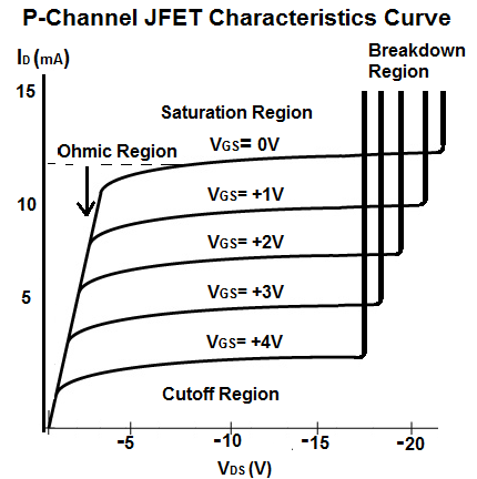
P-Channel JFET Characteristics Curve
The transconductance characteristics curve of a JFET transistor is the the curve which shows the graph of the drain current, ID verses the gate-source voltage, VGS. It represents the gain of the transistior. Gain shows the ratio of the output versus the input. The input is the voltage fed into the gate terminal. The output is the current output by the transistor.
The ratio of change in drain current, ∆ID, to the change in gate-source voltage, ∆VGS, is the transconductance, gm. This is what this characteristic curve serves to show.
The transconductance curve, as for all semiconductor devices, is nonlinear, for most of the curve, meaning changes to VGS do not directly increase or decrease drain current, ID.
Below is the characteristic curve for an P-Channel JFET transistor:
How an P-Channel JFET Works
An P-Channel JFET turns on by taking a positive voltage to the source terminal of the transistor and a gate-source voltage, VGS, between 0V and +4V. It shuts off by taking in a positive gate-source voltage, VGS, above +4V.
You can see based on this P channel JFET transconductance curve that as the positive voltage to the gate increases, the gain decreases. You can see that the gain, the current ID output by the transistor, is highest when the voltage fed to the gate terminal is 0V. As we increase this voltage, again, as stated, the gain decreases.
This transconductance curve is important because it shows the operation of a P channel JFET.
You can also see that the transconductance curve, as for all semiconductor devices, is nonlinear, for most of the curve, meaning changes to VGS do not directly (linearly) increase or decrease drain current, ID, even though this is a lesser issue.
The big point is that, a P-Channel JFET turns on by having a positive voltage applied to the source terminal of
the transistor and ideally no voltage applied to the gate terminal. The transistor circuit
shuts off by taking in a positive gate voltage, VGS, above about +4V or so. The transistor is in its fully
conductive state and is in maximum operation when the voltage at the gate terminal is 0V. As we increase the amount of
positive voltage the gate terminal receives, the transistor becomes less conductive. Once the positive voltage reaches
a certain threshold, the P channel JFET circuit stops conducting altogether across the source-drain terminal.
Regions of the Characteristics Curve
The Regions that make this characteristic curve are the following:
Cutoff Region- This is the region where the JFET transistor is off, meaning no drain current, ID flows through the source-drain region.
Ohmic Region- This is the region where the JFET transistor begins to show some resistance to the drain current ID that is beginning to flow through the source-drain region. This is the only region in the curve where the response is linear.
Saturation Region- This is the region where the JFET transistor is fully operational and maximum current is flowing. During this region, the JFET is On and active.
Breakdown Region- This is the region where the voltage that is supplied to the source terminal
of the transistor exceeds the necessary maximum. At this point, the JFET loses its ability to resist current
because too much voltage is applied across its source-drain terminals. The transistor breaks down and current flows
from source to drain.
If you really want to make sense of all the technical details of the graph above, you have to really that a P-channel normally receives positive voltage to the source terminal of the JFET. So the source terminal receives positive voltage and the drain terminal is normally grounded. So the source terminal is positive relative to the drain terminal. Notice that the voltage on the horizontal of the graph represents the voltage, VDS. VDS is the voltage across the drain and the source, in that order. Since we, again, feed positive voltage to the source terminal and ground the drain terminal, the drain terminal is negative with respect to the source terminal. This is why you see negative voltages for VDS. A negative voltage for VDS just means that we're feeding positive voltage to the source terminal. So if you think of it that way, it makes a lot of sense. If you look all the way to the left of the curve at VDS being around 0V, no drain current can flow because the source terminal needs positive voltage. So if we increase positive voltage to the source terminal which means we're making the drain terminal more negative, we increase the output drain current. About +10V to the source is the midpoint of the graph (which is -10V VDS). And as we go above about +20V or so the source terminal, we reach the transistor's breakdown point.
So this should help to understand a P Channel JFET characteristics curve better and thus a P channel JFET as a whole.