
Paralleling of MOSFET Transistors in Power Electronics Circuits
In this article, we explain why MOSFET transistors are placed in parallel in power electronics devices such as power inverters. This configuration is sometimes referred to as a MOSFET array.
You will see this frequently in power inverter circuits.
After the oscillator circuit (in order to convert the input DC voltage to an oscillating waveform, usually a square waveform) and the MOSFET driver circuit (if needed), there is a usually an array of 2 or more MOSFET transistors in parallel.
This can be seen in the circuit below.
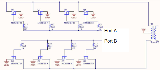
Above you see 4 MOSFET transistors in parallel for each port, with the output from the MOSFET driver circuit feeding each of the ports.
So why is this construction used so frequency in power electronics circuits such as power inverters? What is the reason for this?
In high-power switching applications, transistors can be paralleled to share the load current.
In this construction, though, one must ensure that the current sharing between various parallel transistors is uniform, such that no transistor is over burdened and goes into thermal runaway.
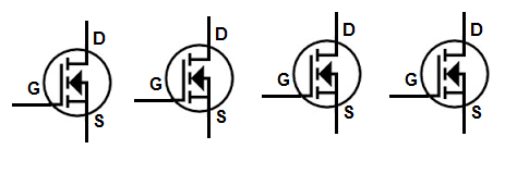
In this construction, each MOSFET transistor needs its own gate resistor with a value from a few ohms up to tens of ohms. This helps with current sharin and prevents gate oscillations.
Parallel MOSFETs are a common way also to reduce conduction losses and spread power dissipation over multiple MOSFETs.
Conduction loss refers to the power that is lost to heat when a circuit is in operation (this can include on, off, and switching states).
MOSFET transistors are physical devices, so they have internal resistance. Even though ideally, there would be absolutely no resistance from drain to source in a MOSFET when the transistor is on the on state (due to sufficient voltage to the gate allowing conduction from drain to source). However, because a MOSFET is a physical device, it does have internal resistance from drain to source even after receiving sufficient power to the gate. This is referred to as RDS(on).
Ohm's law states that I= V/R, so the current is inversely proportional to the inverse of its on resistance.
Also important to note is that no 2 transistors have the same RDS(ON). Transistors are very variable devices. So 2 different transistors will have at least slightly different RDS(ON values. Therefore, the transistor with the lowest resistance value will carry more current. As the current increases through a transistor, heat is generated in the form of power dissipation. This increases the RDS(ON of the transistor.
When working with a particular MOSFET transistor, you should be able to locate its datasheet.
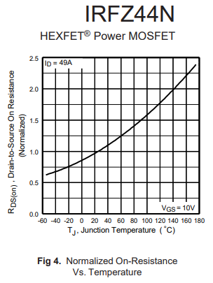
Within this datasheet are various parameters of the transistor, including the maximum drain-source voltage it can manage, the maximum drain current..etc. However, there also exists a graph which is named the Normalized on resistance vs temperature. This shows us a graph of how RDS(ON changes in response to changes in the temperature of the transistor at a specific drain-source voltage and drain current.
Below you can see the Normalized on resistance vs temperature of the IRFZ44N MOSFET transistor, which is a 49A 55V N-channel MOSFET transistor.
If you want to see the entire datasheet for this MOSFET, you can see it here: IRFZ44N N-Channel Power MOSFET Datasheet
So why is this being shown?
This is being shown because as stated before, the transistor with the lowest RDS(ON will carry more current, because current takes the path of least resistance. As it heats up, through power dissipation, its RDS(ON increases; this shifts some of the current to the other FETs, since now its resistance is increasing. This is one way in which current sharing between MOSFETs helps to regulate the thermal properties of the circuit. Thus, the junction temperatures of paralleled FETs will be roughly even. This reduces overall conduction losses of the circuit, because you can see based on the graph there isn't a linear relationship between normalized on resistance and temperature.
In this way, power dissipation is spread out over multiple devices to limit the maximum junction temperature.
These MOSFETs can then be mounted on a common heat sink or copper plane to maintain equal temperatures.
The placement and layout of each MOSFET should be identical and symmetrical to equalize parasitic inductance in the critical gate-to-source and drain-to-source loops.
Of course, whether you need multiple power MOSFETS in parallel for a circuit depends on the power requirements of the circuit. If a circuit is low power, a single FET can definitely be sufficient. This comes at a lower space requirement on the circuit board and less cost. But when working with high power (high voltage and high current), it makes sense and may be necessary for less power loss and greater thermal regulation truly to use multiple power MOSFETs in parallel for greater efficiency (less conduction loss and, thus, power loss) and greater thermal management.
Power inverters working with any decent amount of wattage usually use this parallel MOSFET array for current sharing and greater thermal regulation. Thus, instead of a single MOSFET bearing all the current, it is shared between the parallel MOSFET, since current divides into branches in relation to the resistance of each branch. If all branches are nearly identical, current will be shared nearly equally between all the MOSFETs.
In addition to components such as heat sinks, it is common also that power inverters use fans for thermal control as well, which helps with the thermal control but does add noise to the device.
It is important to note that when working with this setup in order to make the current division as equal as possible between transistors to use the same type of transistor by the same manufacturer to make the transistors as identical as possible. MOSFETs in parallel for better current handling should always be the same transistors.
References Used For This Article
https://resources.pcb.cadence.com/blog/2022-mosfets-in-parallel-improve-current-handling-capability
https://www.ti.com/lit/an/slpa020/slpa020.pdf?ts=1689510483167&ref_url=https%253A%252F%252Fwww.google.com%252F
Related Resources