
How to Build a Potentiometer Circuit with an STM32F407G Discovery Board in C
In this article, we go over how to build a potentiometer circuit with an STM32F407G discovery board in C.
We will show how to incorporate a potentiometer into the circuit, so that we can read the value output by the potentiometer.
A potentiometer is a great useful component because it can output a range of analog values from anywhere from OFF to ON.
This can function for many things, such as dimmer switches.
We will connect this potentiometer to pin PA1 (pin 1 of PORT A).
This is shown in the schematic diagram below.
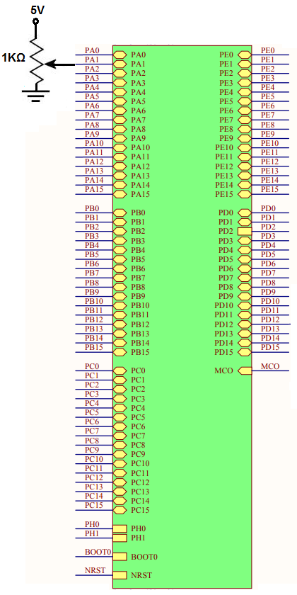
The potentiometer shown in the schematic diagram is a 1KΩ potentiometer, but you could use a potentiometer of any value. It will produce the same results.
We want to be able to get continuous samples from the potentiometer, so we put the code in continuous conversions mode.
Below is the adc.c file, which contains
the functions we need to do an ADC conversion with continuous sampling from the potentiometer.
So we have 2 include statements, which includes header files.
"adc.h" is created by us and we will go over this later.
Next we have a number of macros in our code, which defines a number of registers or values. We will go over these as we use them in our code.
We next define a number of variables. Just like the macros, we will go over these as we encounter them in our code.
We have a function, pa1_adc_init(). This function initializes ADC functionality for pin PA1 of our board.
So in order to perform analog to digital conversion with an STM32F407G discovery board, we have to work with a variety of registers.
One of the first things to notice about all of the ADCs on the STM32F407G board is the bus that they are connected to it, which is the APB2 bus. This is important because we have to enable the peripheral clock of this bus in order to use the ADC component attached to it.
This diagram is shown below.
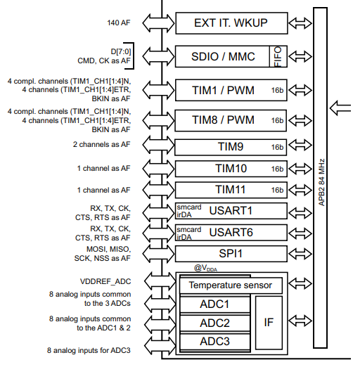
You can see that all 3 ADCs are connected to this bus.
Thus, we must enable the clock of this bus.
This is done through the RCC APB2 peripheral clock enable register (RCC_APB2ENR),
which is shown below.
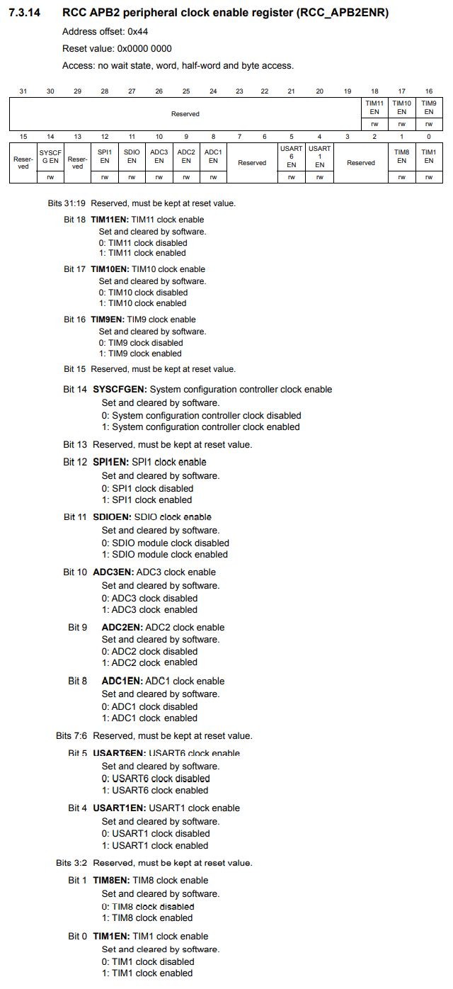
You can see on this register, that you can activate ADC1 by setting 1 to bit 8 activate ADC2 by setting 1 to bit 9, and activate ADC3 by setting 1 to bit 10.
On this register, you can see all of the rest of the components which are connected to the APB2 bus. This register is how you enable any component attached to this bus.
In our project, we will be working with ADC1, so we set 1 to pin 8.
So, with this now, we have activated the peripheral clock for component ADC1.
Next we need to choose a general I/O pin, which will function as an ADC pin. We need to then activate the peripheral clock register for this GPIO port.
We will choose pin 1 of GPIO port A. This is PA1.
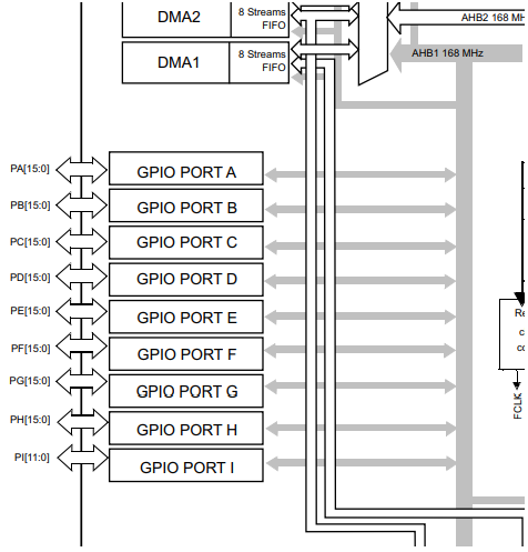
All of the GPIO ports of the STM32F407G board are connected to the AHB1 bus. Therefore, in order to work with a GPIO pin, we need to enable the peripheral clock for the AHB1 bus.
You can see the diagram of this shown below.
So the next thing we have to do is look at the AHB1 peripheral clock register (RCC_AHB1ENR).
This is shown below.
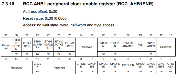
So through this register, we can enable the peripheral clock for any GPIO port. You can see based on the diagram that pin 0 controls GPIO Port A, pin 1 controls GPIO Port B, pin 2 controls GPIO Port C, pin 3 controls GPIO Port D, pin 4 controls GPIO Port E, pin 5 controls GPIO Port F, pin 6 controls GPIO Port G, pin 7 controls GPIO Port I.
In this case, we want to use pin 1 of GPIO Port A, so we enable pin A.
We then must select the mode that the PA1 pin must be in. This is done through the GPIO port mode register (GPIOx_MODER).
This is shown in the diagram below.
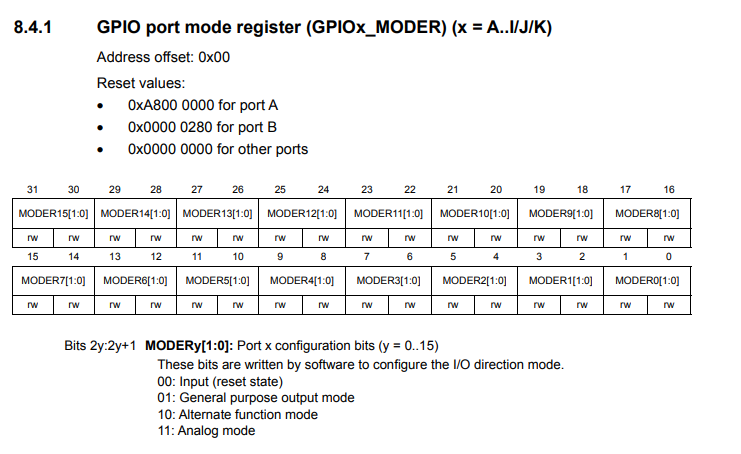
You can see that in order to make a pin analog, we need to write '11' to the pin. In the case of PA1, we need to write a 11 to pins 2 and 3, which is what we do in our code.
Next, we deal with ADC sampling.
So let's say we have multiple ADC devices in our circuit. After all, the board has multiple ADC components (ADC1, ADC2, and ADC3). We can sample up to 3 ADC devices. The ADC regular sequence registers can determine which ADCs we sample and in what order. For example, we can sample ADC2, then ADC3, and then ADC1, and we can even resample from those again.
In our circuit, we only have 1 ADC component, ADC1.
The register we need to deal with in this case is the ADC regular sequence register 3 (ADC_SQR3).
This register is shown in the diagram below.
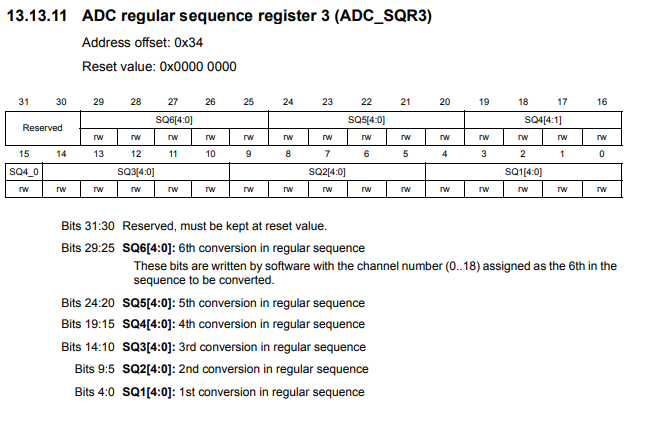
SQ1, the first 4 bits of the register, is the first sequence of the ADC sampling. SQ2 would be if you have another ADC component. SQ3 would be if you have a third ADC component, and so on.
Since we are using ADC1 as the first (the only) sequence, we set bit 0 to 1.
The next thing we need to do is specify the sequence length (how many elements we are doing ADC sampling from).
This is done through the ADC regular sequence register 1. This is shown in the
diagram below.
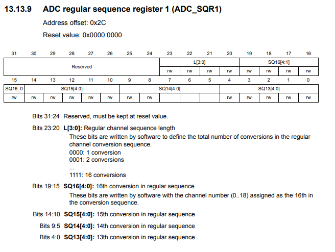
Bits 20 to 23 control the regular channel sequence length. This determines the total number of conversions in the regular channel conversion sequence. In our case, it is 1. Therefore, we set bits 20 to 23 to 0. However, since everything should be 0, we simply set the entire register to 0.
The last thing we must do is enable the ADC, ADC1, in our case.
This is done through the ACD control register 2. This is shown in the diagram below.
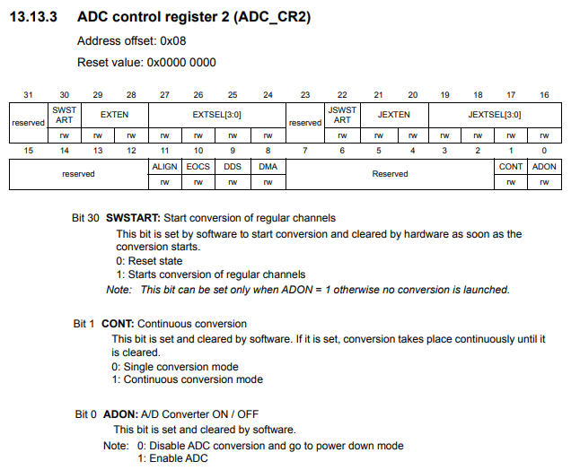
Bit 0 is the ADON bit, which stands for A/D converter ON/OFF. To enable the ADC, a 1 must be set to bit 0.
Next we go on to the next function, adc_start_conversion()
This function actually starts the ADC conversion cycle.
To start the conversion process, we use the ADC control register 2 (ADC_CR2), which is the register shown above.
Bit 30 is the SWSTART bit, which when set to 1 starts the conversion of regular channels.
To sample the value from the ADC component continuously, you would have to set the ADC in continuous mode.
Continuous mode is set by setting 1 to bit 1 of ADC control register 2.
We do this through the line, *pADCCrReg2 |= ADC_CONT_MODE;
This places the ADC in continuous sampling mode.
Our last function, adc_read(), returns the value of the ADC device.
Before we can get the value of the ADC device, we must wait for the conversion to be
complete. We use a while function to check for this. If the conversion is not complete, nothing is
done. If the conversion is complete, we return the value from the ADC data register.
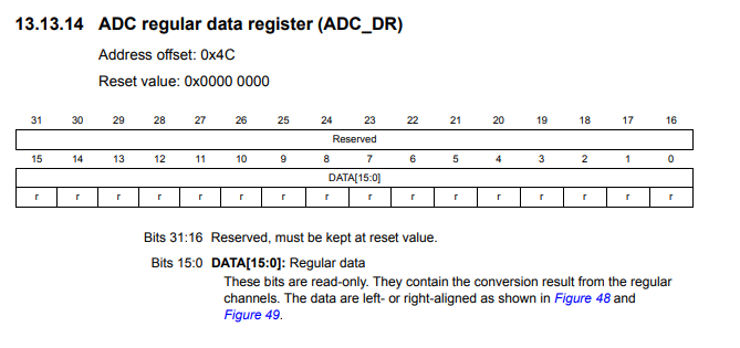
The value that we get from the ADC regular data register is 12 bits, which means it returns values from 0 o 4095 (4096 data sampling points). '
Next we go to our "adc.h" file.
We will include this header file in our main.c file.
Next we have our main.c file, which contains our main() function.
In our main file, we create an integer, adc_value, which is the value returned from the potentiometer in our circuit.
Within our main() function, we initialize our ADC component with the pa1_adc_init() function.
We start the conversion process with the adc_start_conversion() function.
We then have a while(1) function so that we create an infinite loop, since we continuously sample data from the ADC component, the potentiometer.
We read the value into our adc_value variable and then print out the value.
And this is how to build a potentiometer circuit with an STM32F407G discovery board in C.
Related Resources
How to Set Bits of a Number in C
How to Clear Bits of a Number in C