
STM32F407G Microcontroller Clock Tree- Explained
In this article, we explain the clock tree of the STM32F407G microcontroller discovery board.
The clock tree represents the clock structure, or clock hierarchy, of microcontroller board.
Clocks are necessary for microcontrollers, as instructions are carried out with clock signals, either on the rising edge or falling edge. The clock is necessary to provide synchrony so that instructions are carried out at the precise time.
So there needs to be a clock source for a microcontroller.
This clock source can be generated from an internal clock source on the microcontroller board (HSI signal), from an external clock source on the microcontroller board (HSE signal) such as a crystal oscillator, or from a phase locked loop circuit.
This clock signal will be a certain frequency.
The most general clock signal is the system clock (SYSCLK).
This is the clock signal right from the original clock source such as the internal RC circuit or from the crystal oscillator.
The issue is, one clock doesn't fit all.
Just like in a clothing, one size doesn't fit at all. A clothing store doesn't just stock size small. It stocks a whole bunch of sizes to fit different people.
A microcontroller board is the same thing.
One clock frequency doesn't fit all devices.
Some devices need high frequency for operation.
Other devices don't need nearly as much frequency, as they aren't high-speed devices.
Even if a low-speed device could operate with a high-frequency, this may be unnecessary and cause power waste, as high-frequency utilizes higher power than low frequency.
It would be the equivalent to driving a vehicle at the highest gear even when the vehicle is going extremely slow.
This is why on a fairly complex microcontroller board, there is an entire clock structure- in order to be able to feed the right clock frequency to a certain device or pin.
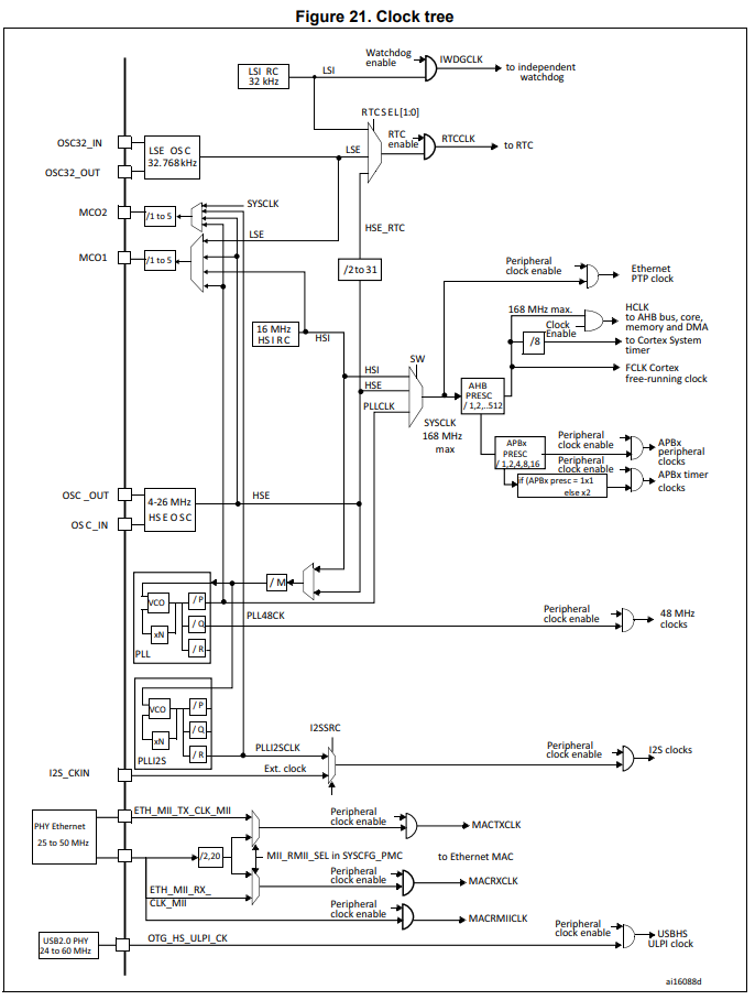
Below is the clock tree diagram for the STM32F407G microcontroller board.
How a clock achieves different clocks for different devices is mostly through prescalers.
Usually the original clock functions as the high range of the clock frequencies used for the microcontroller board.
Then prescalers are used in order to bring the frequency down in ratios of division such as /2, /4, /8, /16, etc.
By default, prescalers are /1, which means it keeps the frequency of the original signal.
There is also a case, where you can increase the original signal. This is done through phase locked loops (PLLs). This is a clock signal that actually can use a multiplier in order to increase the original signal to get a signal of higher frequency.
So, in our clock tree, let's begin with HSI.
If you look for the HSI signal, this is the signal generated internally on the board. You can see this microcontroller board has an HSI signal of 16 MHz generated by the internal RC circuit.
If you follow the signal, it leads to a multipleexr where you see SW, where only one of the clock signals goes to output. At this point, the clock signal is referred to as the system clock, or SYSCLK.
Notice that the clock signal going to the Ethernet PTP clock has no prescalers. It simply is the same as the SYSCLK.
All of the other clock signals have prescalers. This includes the clocks for components such as the AHB bus, core, memory, and DMA, etc.
Within the code, you can configure the values of the prescalers for AHB and APBx buses.
So now you're kind of seeing how the clock structure is working.
Keep in mind the maximum operating frequency of the buses you are using.
For example, the APB1 bus can have a maximum operating frequency of 42 MHz. The APB2 bus can have a maximum operating frequency of 84 MHz.
So you must take your SYSCLK in consideration and prescale it down if it is higher than the maximum allowable frequency for the buses.
So going back before the SYSCLK, you can see that the clock can be either from the originating source of HSI, HSE, or PLLCLK.
The HSE comes from an external oscillator that can be between 4-26MHz.
Lastly, we can have the clock signal original from a PLL, or phase locked loop.
So this is a clock tree for the STM32F407G microcontroller board.
The clock tree
breaks down how the clock signal originates, the path
it travels, and all the prescalers it uses, until it reaches the
target component or pin.
Related Resources