
SYSCLK, HCLK, PCLK1, and PLCK2 Clock Signals in an STM32F4xx Board- Explained
In this article, we explain the various clock signals in an STM32F4xx board, including the SYSCLK, HCLK, PCLK1, and PCLK2 clock signals.
The SYSCLK, HCLK, PCLK1, and PCLK2 clock signals are all clock signals that you will see in the datasheet of an STM32 baord.
The SYSCLK is the main system clock derived from either the HSI clock, HSE clock, or from the PLL clock.
The SYSCLK then branches off to the peripheral clocks, which feed peripheral devices, such as a GPIO port or a UART pin, or a SPI pin, etc.
The first main division of the SYSCLK is the AHB bus (either AHB1 or AHB2). The AHB1 or the AHB2 bus They're both the same clock signal with the same frequency, thus, both buses are referred to as the HCLK.
The HCLK is the clock signal for the AHB bus (AHB1 or AHB2).
This bus then splits into the APB1 bus and the APB2 bus.
The APB1 and the APB2 bus are distinct buses that have different clock frequency capabilities.
The APB2 bus is referred to as the higher-speed bus, which can handle the double the frequency that the APB1 bus can handle. In an STM32F407G board, the APB2 can handle up to 84MHz of frequency. The APB1 can handle up to 42MHz of frequency.
The PCLK1 clock signal is the clock signal that drives the APB1 bus.
The PCLK2 clock signal is the clock signal that drives the APB2 bus.
Below you can see the clock diagram for the STM32F407G discovery board.
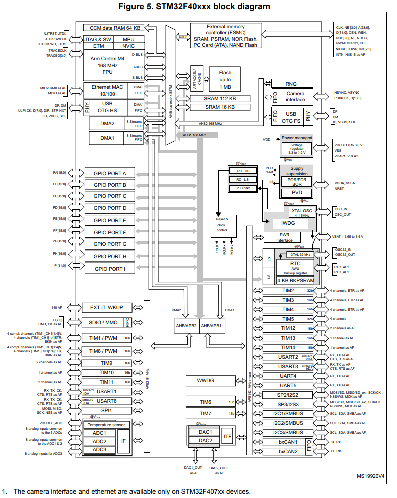
So if you look at this diagram, starting at the top left, where the Arm Cortex-M processor is, you can see that there is an AHB bus stemming from this area. From this AHB bus are AHB1 and AHB2 buses, which all operate at the same maximum frequency of 168MHz. For all essential purposes, the AHB bus is the same as the AHB1 and AHB2 buses (since they all have the same maximum frequency).
The SYSCLK is the clock signal before the AHB bus.
The clock signal after the AHB bus is the HCLK signal.
If you follow the AHB1 bus down, you will see that this bus branches off to a APB1 and APB2 bus.
If you look at the APB1 bus, it can operate at a maximum frequency of 42MHz. So the PCLK1 clock signal is limited to 42MHz.
If you look at the APB2 bus, it can operate at a maximum frequency of 84MHz. So the PCLK2 clock signal is limited to 84MHz.
Another diagram that really helps to illustrate this is the clock tree.
Below is the clock tree for the STM32F407G discovery board.
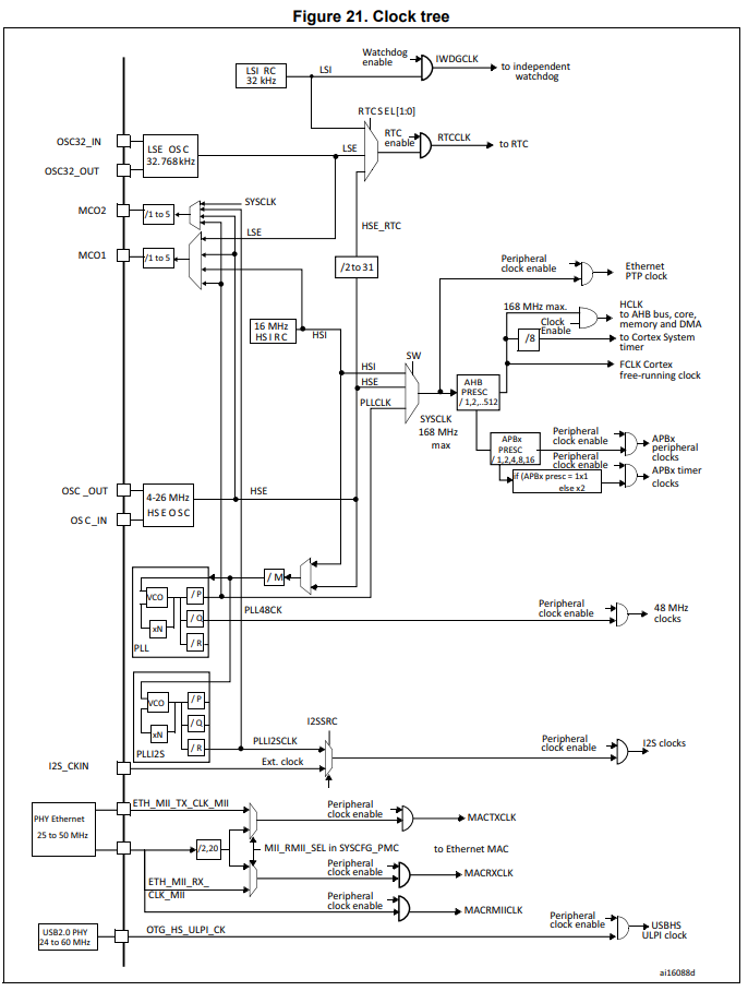
This illustrates the clock signals well.
The SYSCLK is the original clock signal originating from either the HSI, HSE, or PLL clock signals.
The point after the AHB prescaler is the where the HCLK signal begins. This HCLK signal can be the same frequency as the SYSCLK (/1), or it can be a division factor of the SYSCLK (/2, /4, etc.).
After the AHB prescaler, we tehn have the APBx prescaler, which can be used for APB1 or APB2.
If we specify for APB1, this is the PCLK1 clock signal.
If we specify for APB2, this is the PCLK2 clock signal.
So both of these diagram work to explain the SYSCLK, HCLK, PCLK1, and PCLK2 clocks very well.
The SYSCLK and the HCLK have the highest frequency maximums.
Then the PCLK1 clock has the lowest frequency maximum.
The PCLK2 clock then has twice the frequency maximum as the PCLK1 clock.
So this is the SYSCLK, HCLK, PCLK1, and PCLK1 clock signals explained in an STM32F4xx microcontroller
board.
Related Resources