
How to Build a Voltage Amplifier Circuit with a Transistor
In this project, we will show how to build a voltage amplifier with a transistor.
A voltage amplifier circuit is a circuit that amplifies the input voltage to a higher voltage. So, for example, if we input 1V into the circuit, we can get 10V as output if we set the circuit for a gain of 10.
Voltage amplifiers, many times, are built with op amp circuits.
However, with a transistor and the correct biasing, we can produce the same voltage amplification effect of an op amp circuit.
Therefore, in this case, a voltage amplifier is built with all simple, discrete components.
We will show all the components that are necessary to build this circuit as well as how to choose the values of these components. We will also show the maximum gain that a transistor can get based on the values we choose without clipping. So we'll go through all the components of this circuit.
This circuit works as a great voltage amplifier when a more precise and sophisticated op ap IC isn't available or a
simple transistor is preferred.
Components Needed
- 2N3904 NPN transistor
- 1KΩ resistor
- 1.1KΩ resistor
- 4.7KΩ resistor
- 470Ω resistor
- 17μF electrolytic capacitor
- 10μF electrolytic capacitor
The transistor that is chosen can really be any BJT NPN transistor. For this circuit, we choose the 2N3904 transistor.
For a lot of the values of the components we actually compute, you won't be able to find those precise values. For example, below we calculate one of the resistors to be 565Ω. This resistor does not exist. So we approximate the resistor to 470Ω. This resistor value is close enough and is suitable for a replacement value.
A 1.1KΩ resistor also you will not find. So you can either approximate it down to 1KΩ or put a 1KΩ resistor in series with a 100Ω resistor. For all basic purposes, this is not necessary. You can simply connect a 1KΩ resistor instead of 1.1KΩ. It yields similar results.
The same approximations should be used for the capacitor values. Find as close of a value to the calculated capacitor values as possible and use those.
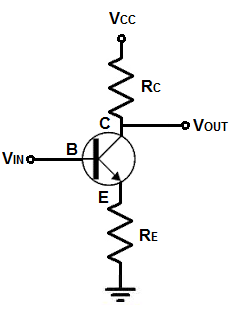
Transistor Voltage Amplifier Circuit
The voltage amplifier circuit that we will build with a BJT NPN transistor and a few resistors and capacitors
is shown below.
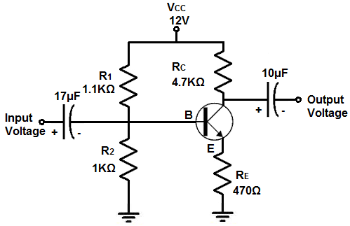
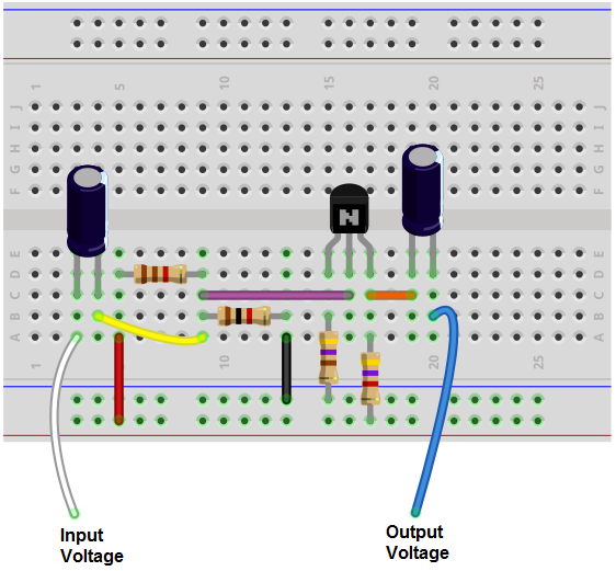
The breadboard circuit of the circuit above is shown below.
So this is our circuit. We will now get into the details of why the various components in the circuit are needed and how to choose the values for them.
So the first thing is we decide how much voltage we're going to supply this circuit. This is the voltage, VCC, applied to the collector of the transistor. You can really choose any value from above VB, the base voltage, to the maximum value that the transistor can handle on the collector. This is typically 40-60V on most transistors. For our circuit, we will choose a reasonable voltage value of 12 for VCC. So this is the first consideration.
Next, now knowing VCC, we bias the base voltage of the circuit, which we means we select the voltage that we want to fall across the base of the transistor. What value do we want across the base? To answer this, we look at the complete picture. The amount of AC voltage that can be present at the output of the transistor is dependent on the DC voltage range that the circuit has. One on end of the spectrum, the transistor can swing up to 12V, which is VCC. On the other end of the spectrum, the transistor can swing down to near ground, about 0.7V. The reason the transistor cannot swing fully to ground is because the transistor will not turn on unless the diode is switched on and that happens at about 0.7V, the barrier voltage for the internal diode. Therefore, 0.7V is the floor of the circuit, and not ground or 0V. Therefore, with a power supply of 12V and a ground 0.7V, the transistor can swing from 0.7V up to 12V. Why this matters in regards to the voltage that we supply to the base is that whatever voltage comes into the circuit has a floor of 0.7V and a ceiling of 12V. Therefore, we want to bias the base voltage so that it falls in between these values. This gives a maximum peak-to-peak excursion for the signal and gives it the most room to operate without clipping. If the base voltage is biased incorrectly or well off the midway, the transistor can have significant clipping that produces poor output. For a 12V ceiling and 0.7V floor, the middle value would be (12 - 0.7V)/2 +0.7V= 6.35V. We have to take the diode voltage drop into consideration because the value at the base is 0.7V higher than at the output. By biasing the base voltage right in the middle of the ceiling and floor, it allows for maximum swing of the AC signal, called maximum peak-to-peak excursion. When biasing a transistor circuit that deals with AC signals, the AC signal that will can appear at the output without clipping is equivalent to the DC biasing. The AC signal will only be able to swing as far as the DC voltage biasing allows it. If the power supply is 20V and the floor is 0.7V, the transistor can swing from a peak value of 20V to a floor of 0.7V. Positioning the transistor at the midpoint of those voltages allows for the maximum swing of the AC signal from the ceiling to the floor. This is the optimum DC operating point for the circuit, called the Q-point or quiescent point. If you select a DC value too low, you will cause the signal to clip earlier at the bottom of the waveform. If you choose a DC operating voltage too high, you will cause the singal to clip at the top of the waveform.
So based on this point, we want the voltage at the base to be midway between 12V, the supply voltage, and 0.7V, which represents the floor. So that the VB= 0.7V + (12V-0.7V)/2, which is 6.35V. So in order to get this voltage, we have to choose our resistors that allows for this voltage to appear at the base. The voltage at the base is biased through 2 resistors. The resistors form a voltage divider and divide the supply voltage. We can divide our supply voltage into any voltage less than the power supply by choosing the correct value resistors. The base voltage, VB= VCC * (R2/R1+R2). In order to solve this equation, we choose the value of one resistor and then based on that resistor value compute the value of the other resistor based on this formula. So for the R2 resistor, a value of 1KΩ is chosen, as a reference point for the other resistor. Plugging these values into the formula, we get VB= VCC * (R2/R1+R2)= 6.35V (12V) (1KΩ). /(R1+1KΩ). Doing the math, this computes to a value of R1= 1.1KΩ. So in order to get a value of 6.35V at the base, the values of the resistors are R1 equal to 1.1KΩ and R2=1KΩ.
Next, we have to decide the value of the RE resistor. The value that we choose is integral so that we do not overheat and possibly destroy the transistor. How we choose RE is based on the value of the current, I E that we want following through the transistor and what is a safe current to flow through the transistor. So we'll just a choose a range that is a safe current that can flow through the transistor that won't burn it out. A safe current is 10mA. That is a decent amount of current and one that will not burn out the transistor. So the emitter resistor, RE= VE/IE, where VE is the voltage across the emitter and IE is the current flowing through the emitter. VE= VB-0.7V = 5.65V. The only difference in voltage between the base voltage and emitter voltage is the diode voltage drop between the 2 junctions. Because the transistor has a diode in it from the base to the emitter, the transistor has an internal voltage drop. Therefore, the emitter voltage is equal to the base voltage minus the voltage drop across the diode. So the formula, RE= VE/IE= 5.65V/10mA= 565Ω. So we will choose an RE value of about 470Ω would suffice well for this circuit, since this resistor is readily available. Across this RE resistor, we can place an optional 100µF capacitor in parallel to the resistor. This acts a generic filter so that any noise on the DC line is filtered out and to ground.
Now we can choose the value of the resistor at the collector, RC. The gain of the circuit is determined by the equation, AV≈ -RC/RE. So we will design our circuit so that we have a gain of 10. This means if we input 1V into the input, we will get 10V as output. So in order to get a gain of 10, RC has to be 10 times larger than RE. Since RE= 470Ω, RC must be 4.7KΩ (10 * 470Ω).
So we have designed the circuit to have a gain of 10.
An important point to note is that if we removed the RE resistor and simply connected the emitter of the transistor to ground, the gain would be higher, because the RE resistance would be lower. However, we include it in our circuit because it provides stability. When we have the resistor at the emitter, the voltage gain depends almost exclusively on the ratio of the collector and emitter resistor, RC/RE. This offsets the intrinsic properties of a transistor, such as the bias current and temperature instability. So the resistance dominates over these intrinsic properties to provides stability. Therefore, it eliminates a lot of unpredictability that can result. So even though it reduces the gain, the stability is improved, so it's worth the compromise. So when making a voltage amplifier with a transistor, a pretty small-valued resistor should be attached to the resistor for stability purposes.
It's also important to note that the signal at the output is inverted. So it will be the same signal as the output but upside down.
You can see based on the calculations that the circuit has a high input impedance and a high output impedance. As we calculated, the output impedance is βRE, which we calculated to be 56KΩ. The input impedance is approximately equal to RC. Therefore, the output imepdance is approximately 4.7KΩ, which is relatively high. Therefore, this circuit will not function as a buffer. Even though it has a high input impedance like a buffer, it has a high output impedance, which will not produce a buffering effect. An op amp buffer or a transistor buffer typically will have an output of just a few ohms, such as 5Ω or less. The circuit we built has an output impedance of nearly 5KΩ. Therefore, unlike a buffer, it won't be able to power on a low-impedance device. This is because the output resistance (or impedance) forms a voltage divider with the load that you attach to the output. Voltage divides. The device that you connect competes with the output resistance. The device with the greater impedance gets the bulk of the output voltage. This is why you want the output impedance of the transistor circuit to be low and the impedance of the output load you connect to be much higher. So that voltage falls across the output device, enough to power it on.
Therefore, with this circuit, as is, it won't be enough to power on a device due to the high output impedance. Therefore, we must connect either connect a buffer to the output of this transistor voltage amplifier circuit or connect an emitter follower to the output, which acts as a buffer. This will then allow an output device to be powered on. You cannot attach an output device directly to the circuit as is, without adding a buffer to the circuit.
Now lastly we have to choose the value of the capacitors in this circuit. Both capacitors have the same function. They allow only the AC signal to pass through and block the DC from passing through. So they function as coupling capacitors.
We'll first show how to calculate the value of the capacitor at the input.
In order to correctly choose an appropriate value of the capacitor, we have to take many things into account, which we will now discuss.
One, we have to decide the cutoff frequency of the circuit. This is the frequency that we want filtered out. If you're dealing with sound signals, the frequency range that is audible to humans is 20Hz to 20,000Hz. If you're building our transistor so that we only want audible signals passed through, 20Hz is a good cutoff frequency to choose. This means that any frequency at that range or lower will be filtered out to ground. So we will choose 20Hz as our cutoff frequency. If we take 20Hz and apply it to angular frequency, ω=2πf, we get ω=2πf≈125s-1. This is one part of the equation.
The next thing we must consider is the value of the resistance that the capacitor sees. The first part of this circuit from the capacitor and the resistor that it sees down to ground forms a high-pass filter, an RC high-pass filter. An RC high-pass filter is a circuit composed of a capacitor with a resistor connected to ground.
If you visualized current flowing into the circuit, current can go either 1 of 3 ways. Current can go through the capacitor and through the R2 resistor and down to ground. Current can go through the capacitor and through the R1 resistor. Or current can flow through the transistor and flow through the RE resistor down to ground. It may seem strange that current can flow through the R1 resistor but AC signals see DC voltage levels as ground as well. So even though it's at the DC level of 12V (through R1), to AC signals, it can also be a ground; this is why this can be a path down to ground as well.
So these are the 3 ways that current can flow in the circuit. EVen though current can take those paths, it's ultimately what a capacitor sees that determines the real resistance that it encounters. So we'll talk about this now. Resistors R1 and R2 are in parallel. Therefore, the capacitor sees the equivalent resistance of these 2 parallel resistors. So the capacitor sees the 1KΩ in parallel with the 1.1KΩ resistor. The equivalent resistance of these resistors is roughly 500Ω. So this the resistance that the capacitors sees at one pathway. The other pathway is when the current goes through the transistor and through resistor RE. This resistance will be βRE. With β equal to about 100, doing this math, this resistance computes to 56KΩ.
Remember that current always takes the path of least resistance. So between the options of 500Ω or 56KΩ, current will obviously take the 500Ω pathway.
So 500Ω is the equivalent resistance that the RC high-pass filter network sees and we know that we want a cutoff frequency of 20Hz. And calculating the angular frequency for 20Hz gives us, ω=2πf≈125s-1.
So going to the equation, REQC1= 1/125s-1= (470Ω)C1= 0.008s. Doing the math, this computes into a C1 value of 17µF. So the first capacitor is 17µF.
Now we move onto the second capacitor. And it's chosen similarly to the first capacitor.
We want the second capacitor to react similarly to the first, in regard to the frequency that we're dealing with. This is because the same frequency signal that is input is output. So you want to match the frequency response for both capacitors to the same frequency. So for the output capacitor, we also calculate it according to its 20Hz frequency response. Computing the angular frequency, we again get, ω=2πf≈125s-1.
We use the same formula again, REQC2= 1/125s-1.
What is REQ in this case? REQ is the resistance that the output capacitor sees. The dominant output resistance that exists is resistor RC, which is 4.7KΩ. So the output resistance is basically this value.
So plugging these values into the equation, REQC2= 1/125s-1= (4.7KΩ)C2= 0.008s. Solving for C2, we get 1.7µF. So this is the value of the output capacitor. We could round this down to 1µF or up to 10µF. It's not that precise. We will round it up in this case because 10µF gives the capacitor more room to operate.
And now we've solved for all the values of the components in the circuit.
So if we input a 1V signal into the input, we get a 10V signal as output.
The output voltage has a ceiling of 12V, so the maximum signal we can get at the output is right under 12V ceiling.
This is because you have to minus the voltage drop. So really the peak voltage output can be up to 11.3V (12V-0.7V) because 0.7V is the floor, not 0V. If you the voltage above this point
exceeds the near 12V mark, there will be clipping of the voltage signal, which produces distortion. Therefore, you have to know the maximum voltage range that is allowed based on the biasing for the
circuit so that you don't get clipping and distortion at the output.
Related Resources
How to Build a Square-to-Triangle Wave Converter Circuit
How to Build a Square-to-Sine Wave Converter Circuit
How to Build a Clock Circuit with a 555 timer
How to Build an Astable Multivibrator Circuit with Transistors
How to Build a Multivibrator Circuit with a 4047 chip (for astable mode operation)
How to Build a Voltage-Controlled Oscillator Circuit with a 4046 Chip
How to Build an Oscillator Circuit with a 7414 Schmitt Trigger Inverter Chip
How to Build a Sine Wave Generator Circuit with a 555 Timer
How to Build a Ramp Generator with Transistors
How to Build a Voltage-controlled Oscillator with a 555 Timer Chip