
What is the Cutoff Region of a FET Transistor?
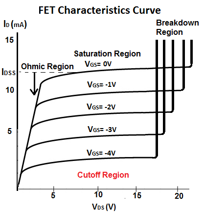
The Cutoff Region of a FET transistor is the region where the drain-source channel resistance is at its maximum and there is no no drain current, ID, flowing from the drain to the source of the FET transistor.
In this region, the transistor is off.
The cutoff voltage (VGS,off), to turn a transistor off, is applied to the gate-source region of the FET transistor. It is the particular gate-source voltage where the JFET acts like an open circuit.
For N-channel JFET, the cutoff region point is reached when the gate-source voltage, VGS, goes below a certain negative voltage. For the JFET above, it is -4V. And for P-Channel JFETs, the cutoff region point is reached when VGS goes above a certain positive voltage, perhaps 4V or so. At this point, the current flowing from drain to source will cease and the transistor turns off.