
What is the Transconductance Curve of a JFET Transistor?
The transconductance cruve of a JFET transistor is the the graph of the drain current, ID verses the gate-source voltage, VGS.
The ratio of change in drain current, ∆ID, to the change in gate-source voltage, ∆VGS, is the transconductance, gm.
The unit of transconductance is the siemen (S). It is the reciprocal of resistnace (Ω).
The transconductance curve, as for all semiconductor devices, is nonlinear, for most of the curve, meaning changes to VGS do not directly increase or decrease drain current, ID.
Below are the transconductance curves of N-Channel JFET transistors and P-Channel JFET Transistors.
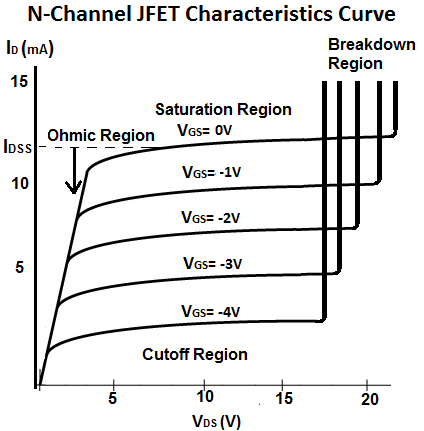
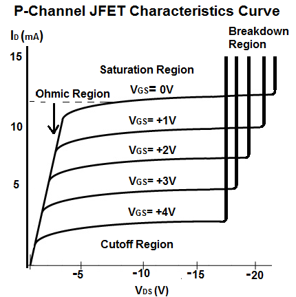
The Regions that make up a transconductance curve are the following:
Cutoff Region- This is the region where the JFET transistor is off, meaning no drain current, I D flows from drain to source.
Ohmic Region- This is the region where the JFET transistor begins to show some resistance to the drain current, Id that is beginning to flow from drain to source. This is the only region in the curve where the response is linear.
Saturation Region- This is the region where the JFET transistor is fully operation and maximum current, for the voltage, VGS, that is supplied is flowing. During this region, the JFET is On and active.
Breakdown Region- This is the region where the voltage, VDD that is supplied to the drain of the transistor exceeds the necessary maximum. At this point, the JFET loses its ability to resist current because too much voltage is applied across its drain-source terminals. The transistor breaks down and current flows from drain to source.