
How to Build a Tri-state Buffer Circuit with a 74HC125 Chip
In this project, we will build a tri-state buffer circuit with a 74HC125 chip.
A tri-state buffer is a buffer that can be in 1 of 3 output states. It's called a 3-state output.
The tri-state buffer can be in a LOW, HIGH, or high impedance state.
So a tri-state buffer is just like a logic chip in that it offers HIGH or LOW states, but it also offers the additional state of high impedance.
Tri-state buffers are mostly used when the outputs of the buffers connect to a common bus that is shared by multiple devices, where the bus cannot listen to more than one device at a time.
When the tri-state buffer is in a high impedance state, the output of a tri-state buffer is removed from the line that it is connected to. So it's as if it is not connected at all. If we do this to all the tri-state buffers save one, the bus can listen to one device at any given time.
So this is why tri-state buffers work really good with their 3-state logic.
They're also used in registers and flip flops, so they appear a lot in computer memory and processors.
Each tri-state buffer of the 74HC125 has 2 inputs, an output enable and the data input. If the output enable is disabled, this puts the buffer in a high-impedance state. If the output enable enable is enabled, then the load can be driven either to a HIGH or LOW state. If the input is HIGH, the output will be HIGH. If the input is LOW, the output will be LOW.
In this circuit, we will simply connect a tri-state buffer and show how it works with manual pushbutton control.
The tri-state buffer isn't used for a real-life purpose as it would be done; this circuit simply just shows
how it works.
Components Needed
- 74HC125 Tri-state Buffer Chip
- 2 Pushbuttons
- LED
- 470Ω resistor
The 74HC125 chip is a quad tri-state buffer chip. This means it contains 4 independent tri-state buffers.
The 74HC125 chip can be obtained very inexpensively (under $0.50) and it's available from a number of different online retailers. One place to find is at Tayda Electronics at the following link: 74HC125 Tri-state Buffer IC.
The datasheet for the 74HC125 is shown at the following link: 74HC125 Register Datasheet.
The 74HC125 is a 14-pin chip.
The pinout for the 74HC125 is shown below.
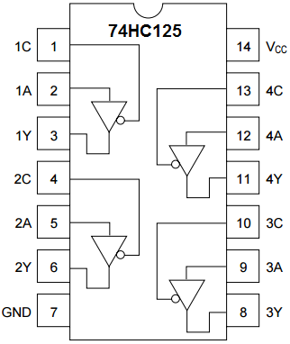
To power the 74HC125, we connect positive voltage to VDD, pin 14, and we connect GND, pin 7, to power ground.
The 74HC125 chip has 4 independent tri-state buffers.
Each tri-state buffer has 3 pins associated with them- 2 input pins and 1 output pin. So this makes up 12 of the 14 pins of the chip.
In order for the output of a tri-state buffer to be able to turn on, the output enable pin must be HIGH and input pin must be HIGH. Only if these conditions are met does the output go HIGH.
The output enable pin enables output. It is labeled C on the inputs of the tri-state buffers. It is an active LOW pin. When LOW, outputs can go HIGH or be on. When HIGH, outputs cannot turn on and are in a high impedance state. This essentially cuts it off the output from the bus it is connected to.
The input, labeled A, determines the output. If the output enable is enabled, if A is HIGH, the output is HIGH. If A is LOW, the output is LOW.
This logic is shown in the table below.
| Tri-state Buffer Logic (3-state Logic) | ||
| Input (A) | Output Enable (C) | Output |
| X | 1 | Z (High impedance) |
| 1 | 0 | 1 |
| 0 | 0 | 0 |
X stands for "does not matter". And Z stands for "high impedance".
74HC125 Tri-state Buffer Circuit
The schematic diagram of the 74HC125 tri-state buffer circuit we will build is shown below.

To power the 74HC125 tri-state buffer chip, we feed 5V into VCC, pin 14 and we connect GND, pin 7, to power ground. This establishes power to the 74HC125.
For this circuit, we're just using a single tri-state buffer.
We connect the 2 inputs of the tri-state buffer to pull-down resistors. So when the pushbutton is unpressed, the 2 inputs are in LOW logic state. When we press down on the pushbuttons, the logic state of the pins is now HIGH.
Pin 1 is the output enable pin, labeled C on the pinout. This pin is active LOW. So it must be LOW in order for the output, which is an LED, to turn on. If it is HIGH, the output will be in a high impedance state. If it is LOW, then the output can be driven to a HIGH or LOW state. So in order for the LED to turn on, this button must be pressed.
Pin 2 is the data input pin, labeled A on the pinout. When the output enable pin is LOW, this pin determines the logic state of the output. If this pin is LOW, the output will be LOW. If this pin is HIGH, the output will be HIGH.
Pin 3 is the output pin. To this pin, we connect the output device; in this case, it's an LED. We attach a 470Ω resistor to limit current to the LED so that it doesn't burn out.
How the Circuit Works
How the circuit works is only both pushbuttons are pressed down does the output, which is the LED, turn on.
If we don't press down on the pushbutton attached to pin 1, the buffer will be in a high impedance state. If this button is not pressed, it does not matter whether we press the input button or not. If the output enable is disabled, the input pin has no effect.
Now if we press down on the output enable pushbutton, enabling the output, and we don't press down on the input pushbutton, the output will be in a LOW logic state. Still, the LED will not turn on, because the LED will be connected to ground on both sides, so there's no electrical potential to power on the LED.
With the output enable still enabled, if we push down on the input pushbutton, the output will be in a HIGH logic state. The LED now turns on because there is electrical potential
across the LED. One terminal is connected to 5V and the other to ground.
And this is how a tri-state buffer circuit can work with a 74HC125 chip.
Related Resources
How to Build a Register Circuit with a 4094 Chip
How to Cascade 4094 Registers
How to Build a Shift Register Circuit with a 74HC595 Chip