
How to Cascade 4094 Registers
In this project, we will cascade 2 4094 registers together so that we can double the amount of bits that can be stored.
The 4094 register is a 8-bit register, meaning it can hold up to 8 bits of data.
However, if you need more than 8 bits of storage, a good solution is to cascade registers together. If we cascade 2 4094 registers together, we get double the storage. Instead of being able to only store 8 bits of data, we can store 16 bits of data. If we add a third 4094, we can store 24 bits of bits. If we cascade a fouth 4094, we can store 32 bits of data. So for each additional 4094 register that we can cascade, we gain an extra bits of data.
Pretty much all registers have a way for other registers (of the same type) to be cascaded. This is because the data storage that one register may allow may not be sufficient in all cases. The user can then have the ability to cascade additional registers to meet storage demand.
In this circuit, we will simply show how to cascade one additional 4094 register. Once you know how to cascade one, you will know how to cascade how ever many you may need to. It's the same for each additional cascade.
Cascading registers is pretty important because you can get any amount of storage you need from registers.
You can keep cascading until you have enough storage for whatever purpose you're using it for.
Components Needed
- 2 4094 CMOS Register Chip
- 16 470Ω resistors
- 18 LEDs
- 2 Pushbuttons
- 2 1KΩ resistors
- Clock source
The 4094 chip is a CMOS register chip. A register is a chip that can store 8 bits. These 8 bits show up at the output pins. If the bit is LOW, an output device such as an LED will be off. If the bit is HIGH, an output device such as an LED will be on.
The 4094 chip can be obtained very inexpensively (under $0.50) and it's available from a number of different online retailers. One place to find is at Tayda Electronics at the following link: 4094 CMOS Register IC.
The 4094 is a 16-pin chip.
The pinout for the 4094 is shown below.
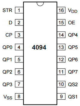
The 4094 works from voltage anywhere from 3V-15V. So we feed this voltage into VDD, pin 16 and we connect VSS to ground.
Pin 1 is the STROBE input. This input must be placed HIGH to transfer bits to the storage register. If this pin is LOW, no data can be transferred to the storage register so they won't appear at the output.
Pin 2 is the data input. Depending on whether this pin is HIGH or LOW determines whether a 1 or 0 gets shifted into the register.
Pin 3 is the clock pin. The 4094 chip needs a clock signal in order to operate. Data gets shifted into the storage register on the rising edge of the clock signal.
Pin 15 is the Output Enable pin. This pin must be HIGH in order for the output pins to go HIGH. If this pin is LOW, outputs are disabled.
Pin 9 and 10, QS1 and QS2, are used for cascading a number of 4094 chips together. QS1 would be used to transfer data serial from one chip to the next on the positive edge of a clock signal with a clock that is high speed. QS2 would be used for transferring data serially from one chip to the other on the falling edge of a clock signal with a clock that is slow speed. So if you are cascading chips together, you either connect the QS1 or the QS2 pin to the data input pin of the second 4094 chip. This allows the shifting of data from one register chip to the next.
QP0-QP7 are the output pins. To these pins, we attach our output device we want to turn on when a 1 is
shifted to that pin.
Cascaded 4094 Register Circuit
The schematic diagram of the cascaded 4094 register circuit we will build to drive on LEDs is shown below.
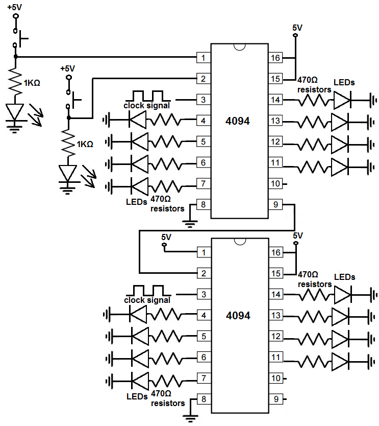
To power the 4094 register chip, we feed 5V into VDD, pin 16 and we connect VSS to ground. This establishes power to the 4094.
We connect the strobe input and the data input of the first 4094 to a pull-down resistor. These pins will normally be LOW when the pushbutton is unpressed. So they have a value of 0 when unpressed. When we press down on the pushbutton, the value of the pin goes HIGH or to 1. We attach an LED to the pull-down resistor just to serve as a visual indication that the pushbutton has been pressed and it has registered.
We connect the strobe input of the second 4094 register permanently HIGH. This is because we always want it to accept the input from the first shift register. So we just keep it activated.
To pin 3, the clock pin, we have to connect a clock signal, a digital square wave signal. This clock signal is connected to both 4094s. A clock signal can be obtained from a number of sources such as from a function generator if you have one. A function generator can be put in square wave mode in which case it can function as a clock. A clock can be obtained from a 555 timer circuit in astable mode. A clock can be built with a 4047 multivibrator circuit in astable mode. A clock circuit can be built with a 7414 schmitt trigger inverter. It can also be built with a 4046 phase locked loop. So there are many ways of producing a clock signal.
Pin 15 is the Output Enable pin. In order for the outputs to be able to turn on, this pin must be connected HIGH. Since you do not want to turn on this feature at any point in our circuit, we simply connect it permanently HIGH to VDD on both 4094 chips.
Pin 9 and 10, QS1 and QS2, the pins for cascading multiple 4094s together. We connect QS1, pin 9, of the first 4094 register to the data input, pin 2, of the second 4094 register. We leave QS2, pin 10, unconnected, since only one is needed for cascading to be in effect. By connecting QS1 to the data input of the following register, we allow for high-speed operation on the rising edge.
QP1-QP7 are the 8 output register bits for each register, so there are 16 outputs in total between the 2 chips. To these pins, we connect an LED along with a current-limiting resistor so that the LED doesn't burn out from excess current. If the output is LOW, the LED will be off. If the output is HIGH, the LED will be on.
For the second register 4094, the QS1 and QS2 pins are left unconnected, because we are not cascading a third register chip.
These should always be left unconnected, as opposed to connected to ground, because voltage is still present on these pins, so you don't want to short them
to ground.
How the Circuit Works
So these circuit is mainly controlled by 2 inputs, the strobe input pin and the data input pin, pins 1 and 2.
Being that the Output Enable (OE) pin is tied permanently HIGH, the output is always enabled, so we don't have to worry about that pin.
The strobe and data inputs are normally LOW.
To shift data to the storage register, we have to send a HIGH signal to the strobe input and then the data is shifted into the storage register. So if we are sending a 0 to the storage register, we simply press down on the strobe input and release it. This shifts a 0 into the storage register. If we want to shift a 1 in to the storage register, we press down on the data pushbutton; this makes it HIGH or 1. Then we press down on the strobe pushbutton. This shifts in that 1. And we can do this as many times as we want. Each time we do it, another bit gets shifted in. And this is how we can get our 8 bits to the values we desire. Once they are shifted in, you will see them appear at the outputs as either the LED being on or the LED being off.
When the 8 bits have been reached, with each additional bit shifted in to the first register, a bit gets shifted to the second register. In total, 16 bits can be shifted in.
And this is how a 4094 register operates.
Related Resources
How to Build a Register Circuit with a 4094 Chip