
How a PNP Transistor Works

A PNP transistor is a bipolar junction transistor (BJT). A BJT is a transistor that is current-controlled and allows for current amplification.
In this article, we will go over exactly how a PNP transistor works so that you can know how to power it in a circuit to allow for amplification and/or switching.
How a PNP Transistor Works
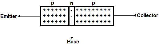
A PNP transistor is a transistor which is made up of 3 regions, the base, emitter, and collector. The collector and emitter regions are made up of p-type material, which means they are predominately composed of holes. Holes are deemed as positive charges. The base region is made up of n-type material. It is predominately composed of electrons.
Below is a visual diagram of the construction and composition of a PNP transistor.
In order for current to flow from the emitter to the collector, the transistor must be biased in the
following way, shown below:
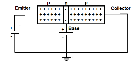
A PNP transistor is a semiconductor. A semiconductor is in an intermediate state between a conductor, which allows for the free and easy movement of electrons and an insulator, which offers great resistance to the flow of electrons. However, if a semiconductor is biased properly, meaning voltage is allocated appropriately to the parts of a transistor, then a great amount of current can flow. This is what we are doing now, we are biasing the transistor so that current can flow. But to know how to properly bias the transistor, you must know how the transistor is internally constructed.
As stated before, a PNP transistor is made up of 2 layers of p materials, holes, representing positive charges, sandwiching a middle layer of n material, made of electrons, negative charges. The end goal is that we want to bias our circuit so that current flows across from the emitter to collector to power the load connected to the collector terminal.
Bipolar junction transistors, including the PNP transistor, are made so that current should flow from the emitter to the collector region. The collector region is the largest region which contains the most charge. Therefore, this is why we want current to go from the smaller emitter region to the larger collector region, where the most charge is. This is why the collector region is the destination point. It will give out slightly more amplified current than the emitter region. This is wh we connect the load we want to power to the collector side, not emitter.
So we want to bias our circuit so that current flows from the emitter to the collector.
In order to understand how a transistor, there is basically one physics law to understand and that is the law of charges. If you know this, you can figure out how a transistor works. And this is a very simple concept. It is the concept that like charges repel each other and opposite charges attract each other. This means 2 positive charges will repel each other and 2 negative charges will repel each other, while opposite charges will attract each other. This is all you need to know to understand transistors.
The emitter region of a PNP is made up of P material, which are holes. And we want current to flow from the emitter to the collector region. Therefore, we place positive voltage to the emitter region. This makes the holes in the emitter region be repelled by the positive charges. Therefore, current flows downward toward the collector.
The next region we must bias is the base region, the most important region for controlling the on-off capability of the transistor. When no current is going into the base region of a PNP transistor, the base region is very small and offers no real impedement to the flow of current. Thus, current can easily flow across from emitter to collector. This is because without current flowing, electrons are not going into the N-material of the base region. Just think, the base region of a PNP transistor is made up of N material, electrons. If we add more electrons, by allowing current to go in (current is the flow of electrons), we increase or thicken the base region, increasing the barrier between the emitter and collector region, blocking current flow. This is why when we give current to the base, it blocks the flow of current from the emitter to the collector. And when we have no current flowing into the base, current easily flows from emitter to collector. So if we want our to transistor to be fully on, we make sure that the base is connected to ground. This ensures tha no current flows into the base.
The last region to bias is the collector region. This simply just connects to ground, because the positive voltage pushing from the emitter side downward is really all that is needed to produce current flow through the transistor, if there is no base current.
So to connect a PNP transistor to power on a load, all we need is the following circuit:
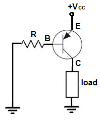
Again, just make sure that the base connects to ground and that there is sufficient positive voltage to the emitter terminal to power the load.
The PNP transistor will not work unless the base is connected to ground. And it cannot be connected to ground directly through a jumper wire. A resistor must be in
place between the base and ground. This makes current flow from the base of the transistor down to ground. The PHP transistor must have negative current flow from the base in order to operate, meaning
current must flow from the base to ground. The base must be sufficiently more negative than the emitter for the PNP transistor to operate.
Related Resources
How to Connect a Transistor as a Switch in a Circuit
How to Connect a (NPN) Transistor in a Circuit
Types of Transistors
Bipolar Junction Transistors (BJTs)
Junction Field Effect Transistors (JFETs)
Metal Oxide Semiconductor Field Effect Transistors (MOSFETs)
Unijunction Transistors (UJTs)
What is Transistor Biasing?
How to Test a Transistor