How an NPN Transistor Works
An NPN transistor is a bipolar junction transistor (BJT). A BJT is a transistor that is current-controlled and allows for current amplification.
In this article, we will go over exactly how an NPN transistor works so that you can know how to power it in a circuit to allow for amplification and/or switching.
How an NPN Transistor Works
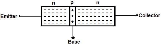
A NPN transistor is a transistor which is made up of 3 regions, the base, the emitter, and the collector. The collector and emitter regions are made up of N-type material, which means they are predominately composed of electrons. Electrons are negative charges. The base region is made up of P-type material. It is predominately composed of holes. Holes are deemed as positive charges.
Below is a visual diagram of the construction and composition of an NPN transistor.
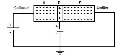
In an NPN transistor, current flows from the collector to the emitter. In order for current to flow from the collector to emitter, the transistor must be biased in the
following way, shown below:
A NPN transistor is a semiconductor. A semiconductor is in an intermediate state between a conductor, which allows for the free and easy movement of electrons and an insulator, which offers great resistance to the flow of electrons. However, if a semiconductor is biased properly, meaning voltage is allocated appropriately to the parts of a transistor, then a great amount of current can flow. This is what we are doing now, we are biasing the transistor so that current can flow. But to know how to properly bias the transistor, you must know how the transistor is internally constructed.
As stated before, an NPN transistor is made up of 2 layers of N materials, electrons, representing negative charges, sandwiching a middle layer of P material, made of holes, positive charges. The end goal is that we want to bias our circuit so that current flows across from the collector to emitter to power the load connected to the collector terminal.
In order to understand how a transistor, there is basically one physics law to understand and that is the law of charges. If you know this, you can figure out how a transistor works. And this is a very simple concept. It is the concept that like charges repel each other and opposite charges attract each other. This means 2 positive charges will repel each other and 2 negative charges will repel each other, while opposite charges will attract each other. This is all you need to know to understand transistors.
The emitter region of an NPN is made up of N material, which are electrons. We want current to flow from the collector to the emitter region. Therefore, we place positive voltage to the emitter region. The electrons in the collector terminal are repelled by this voltage. Therefore, current will flow downward toward the emitter.
The next region we must bias is the base region, the most important region for controlling the on-off capability of the transistor. When no current is going into the base region of an NPN transistor, the base region is large and offers strong resistance to the flow of current. Thus, current does not flow across from the collector to the emitter. This is because the P material comprising the base region, made up of holes, provides a strong barrier separating the collector and emitter regions. However, when current flows into the base, electrons flow into the P material, depleting the amount of holes in the base region. The base region barrier becomes depleted, becoming smaller, until there are enough electrons filling it to completely break down the barrier. When this occurs, current can easily flow from collector to emitter.
The last region to bias is the emitter region. Since current flows from the collector to the emitter, the emitter simply connects to ground, to supply a return path for current in the circuit. So the full path of current starts at the voltage source connected to the collector terminal and ends at the grounded terminal of the emitter and then starts again at the collector terminal.
So to connect an NPN transistor to power on a load, all we need is the following circuit:
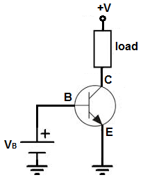
To turn on the transistor, just apply sufficient base current. To turn off the transistor, remove the base current.
Related Resources
How to Connect a Transistor as a Switch in a Circuit
How to Connect a (NPN) Transistor in a Circuit
Types of Transistors
Bipolar Junction Transistors (BJTs)
Junction Field Effect Transistors (JFETs)
Metal Oxide Semiconductor Field Effect Transistors (MOSFETs)
Unijunction Transistors (UJTs)
What is Transistor Biasing?
How to Test a Transistor