What is BVDS of a FET Transistor?
BVDS of a FET transistor is breakdown voltage, which causes the transistor to enter the breakdown region; this the region where the transistor receives too much voltage across its drain-source terminal, which causes the drain-source terminal to break down, which, in turn, makes the drain current, ID, drastically increase.
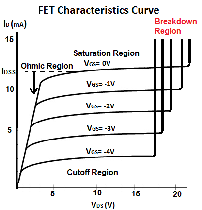
The breakdown region, which the breakdown voltage BVDS causes the transistor to enter, is the last section (to the right) of the FET characteristics curve. In this region, the drain-source voltage, VDS increases too much for the channel to handle. At this point, the FET loses its ability to resist current because too much voltage is applied across the drain-source terminal.
The breakdown voltage, BVDS, occurs typically when VDS rises above anywhere above 17V. The farther the gate-source voltage, VGS, supplied to the transistor, is from the 0V, where the maximum drain current ID occurs, the lower the breakdown voltage is to enter the breakdown region.