
How to Build a Buffer with a NAND Gate Chip
In this project, we will show how to build a buffer with a NAND gate chip.
The chip we will use is the 4011 NAND gate.
We only need 2 NAND gates in order to construct a buffer.
A NAND gate is really a universal chip in that it can create any type of gate possible.
This article just goes to show how to create a buffer from NAND gates. It doesn't go into full detail about the use of buffers. If you want to know why buffers are important and useful in circuits, see How to Build a Buffer Circuit with a 4050 Buffer Chip. this goes into full detail on why buffers are crucial to many types of circuits.
For this circuit, we simply show to turn NAND gates into a buffer so that it functions just like a buffer.
Components Needed
- 4011 NAND Gate Chip
- Jumper Wires
- 470Ω resistor (Optional)
- LED
The 4011 NAND chip is a chip that is very cheap and easily attainable. It can obtained for under $0.50.
The 4011 is a quad NAND gate, meaning it is composed of 4 independent NAND gates.
The 4011 buffer has 14 pins.
The pinout of the chip is shown below.
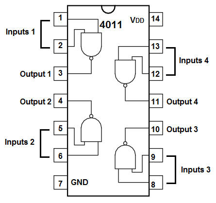
VDD, pin 14, and GND, pin 7, are the power pins for the 4011 chip. VDD receives the positive voltage, while GND is connected to the power supply ground. The chip can be powered up to 20V.
The other pins are for the NAND gates. Being that there are 4 NAND gates and each NAND gate has 2 inputs and 1 output, this
makes up the other 12 pins on the 4011.
The truth table for NAND gate logic is shown below.
| NAND Gate Logic | ||
| Inputs | Output | |
| 0 | 0 | 1 |
| 0 | 1 | 1 |
| 1 | 0 | 1 |
| 1 | 1 | 0 |
Since a buffer has a single input, we tie the 2 inputs together from the first gate so that it's one input. Since the input can either be 2 0s or 2 1s.
When the input is 2 0s, the output is a 1.
When the input is 2 1s, the output is a 0.
By tying the inputs together on a NAND gate, we naturally form an inverter circuit.
By connecting 2 inverters together, we produce the original signal and have created a buffer.
So now that you know all the connections for the 4011, we can show how to build the
buffer from it.
Buffer Circuit
The buffer circuit we will build that buffers a voltage divider circuit is shown below.

The breadboard circuit of the circuit above is shown below.
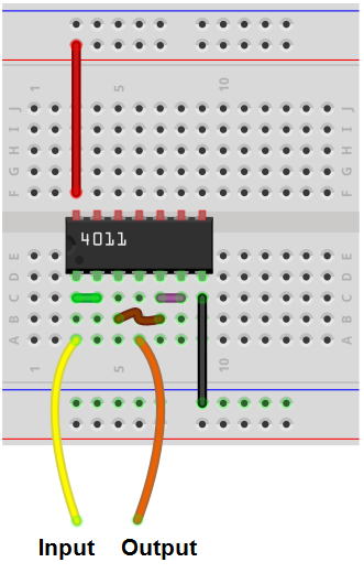
So to power the 4011 NAND gate chip, we give 5V to VDD, pin 14, while connecting GND, pin 7, to the ground of the power supply. This establishes sufficient power to the chip of the 4011. At the same time as providing power to the chip, it is also used for biasing the chip. When the chip's output is LOW, the output is at the level of GND. When the chip's output is HIGH, the output is at the level of VDD, which in this case is 5V. Whatever value you want the output to reach when outputting a HIGH logic state should be placed into VDD, pin 14.
So, for the first NAND gate, we tie the inputs common. So pins 1 and 2 are connected together via a jumper wire. This makes the NAND gate an inverter. Since both inputs are tied common together, the inputs can either be 2 0's (2 logic LOWs) or 2 1's (2 logic HIGHs). If the input is a logic LOW (0), the output after the first gate will be HIGH (1), according to NAND gate logic. If the input is a logic HIGH (1), the output after the first gate will be a LOW (0).
We then make another inverter out of the second NAND gate, again by tying both inputs common together. This inverts the inverted signal from the second signal, making the output signal from the second gate the original signal fed into the input of the first gate.
This allows the circuit to act as a buffer.
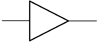
A buffer is a single-input, single-output device.
The output outputs the same signal that is input into it.
Being that the output is the same as the input, how we construct a buffer with a NAND gate is by first making the NAND gate an inverter. We then create a second inverter. The output of the first inverter feeds into the input of the second inverter. Being that the original input signal gets inverted twice, it produces the original signal as output.
This is the simplest way to produce a buffer with NAND gates.
What you see above is 2 NAND gates configured to be inverters.
2 inverters connected together create the original signal.
If you were to take an oscilloscope and place one probe at the input and another probe at the output, you should see that both signals are the same, in amplitude, phase, and everything. If you place the oscilloscope at midway point, which is between the 2 NAND gates which would be at the output of the first gate or the input to the second gate, you should see an inverted signal.
Any signal applied to the input greater than 1/2 of the voltage supply is interpreted as a HIGH signal (1). Any signal applied to the input less than 1/2 the supply voltage is interpreted as a LOW signal (0).
So if we apply 5V to the input, we should get 5V as the output. Now if you were to place a DC voltmeter in between the 2 NAND gates, you should get near 0V. This is because the first NAND gate is an inverter. The inversion of a HIGH signal is a LOW signal, which is near 0V. But since the 2nd NAND gate is an inverter as well, you get 5V from the second NAND gate.
If we apply near 0V (or less than 2.5V to the input), we should get near 0V as the output. If you were to place a DC voltmeter in between the 2 NAND gates, you should get 5V, which is the supply voltage. But the second NAND inverts this and you get near 0V as the final output.
If you don't have an oscilloscope or multimeter, you could check the circuit visually through an LED. You can place an LED at the output and see how it reacts to changes to the input voltage. You should see that when a HIGH voltage is placed at the input, the LED turns on. And when a LOW voltage is placed, the LED is off. Always accompany the LED with a current-limiting resistor as to safeguard it from excess current.
And this is how a buffer can be built with NAND gates such as with a 4011 chip.
Related Resources
How to Build a Buffer Circuit with a 4050 Chip
How to Build a Transistor Buffer Circuit
When a Circuit Needs Buffering