
How to Build a Buffer Circuit with a 4050 Buffer Chip
In this project, we will show how to build a buffer circuit with a 4050 buffer chip.
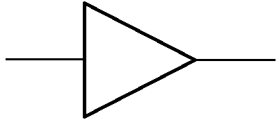
A buffer is a circuit that produces the same voltage output that is input into it.
It may seem useless, since you are getting the same signal back out but buffers are actually very valuable.
In this article, we will explain the full use of buffers and why they are so important for many different types of circuits.
In fact, many people are confused about buffers in general. The general consensus seems to be, if you are getting the same signal output that is input, then why is it needed?
We will go through real-life circuits where buffers save the circuit and allow the circuit to work when it wouldn't be able to do so without it.
The reason buffers are so important is because they have a high-impedance input while having a low-impedance output. The high input impedance allows the full voltage to fall across the buffer. The low output impedance allows whatever load is connected to the buffer to be able to powered on with sufficient power.
You're not going to understand what is written above until explained below in full
detail. You really do have to see real-life example circuits to understand the principle
of why buffers are so important. We'll do so below.
Components Needed
- 4050 Buffer Chip
- 4KΩ resistor
- 6KΩ resistor
- 470Ω resistor
- LED
The 4050 buffer chip is a chip that is very cheap and easily attainable. It can obtained for under $0.50.
It is referred to as a hex, noninverting buffer.
It is called hex because it is made up of 6 separate, independent buffers.
It is called noninverting because it doesn't invert the signal. If it did, it would be an inverting buffer.
The 4050 buffer has 16 pins.
The pinout of the chip is shown below.
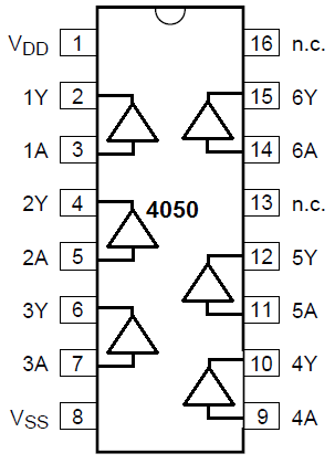
2 of the pins are the power pins. These are VDD, pin 1, and VSS, pin 8. VDD receives the positive voltage and VSS is connected to ground. The supply voltage that can be given can be up to 18V. This establishes power for the chip.
2 of the pins are NC, which stands for Not Connects. They don't get connected in any way.
And the last 12 pins are inputs and outputs for each of the buffers of the 4050. Since there are 6 buffers, there are 6 inputs and 6 outputs.
Looking at the diagram above, the A's represent the inputs of the buffers. And the Y's represent the outputs of the buffers.
For our circuit, we will simply use one buffer. Once you know how to use one buffer, you will know how to use any of the others.
So now that you know all the connections of the 4050, we can go into the heart of why a buffer is such a useful
component.
What is the Point of a Buffer? What's the Purpose of a Buffer?
So now you go into the heart of why you would use a buffer and the cases where it's necessary to have a buffer.
To understand a buffer, we can use nothing else than a voltage divider circuit to illustrate its crucial use.
Let's say that we have a 5V DC source, and you only want 3V from the 5V DC source.
The easiest and simplest way probably to achieve this is to use a voltage divider composed of 2 resistors in series.
The only factor that you have to take into account for voltage division are the values of the 2 resistors.
Because the resistors are in series, the current going through both of them is the same. Therefore, the only thing that differentiates the 2 components are the resistance values. Since voltage, v=IR, where I is current and R is the resistance. Since the current is the same through both components, the only component that has an effect directly on the voltage is the resistance.
The formula to find out the voltage drop in between the components is V= VSOURCE (R2/R1 + R2), where VSOURCE is the supply voltage, R1 is the first resistor on the top and R2 is the second resistor on the bottom.
So to produce 3V at the middle of the 2 resistors, we use a 4KΩ and a 6KΩ resistor. Doing the math, we get V= 5V(6KΩ/6KΩ+4KΩ)= 3V.
So now we have 3V at the middle of the resistor terminal.
Now let's say that we connect a load directly to this 3V, in between the middle of the resistors.
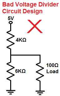
This is a bad design and will not work.
This is because once we add an output device to the circuit which is a load that carries a certain amount of impedance, this changes the circuit and not enough voltage will go to the load.
This is because there is a voltage divider circuit now between the 4KΩ resistor with the 6KΩ resistor in parallel with the 100Ω load resistance. Therefore, the voltage across the output device is now very low. The formula to calculate the equivalent parallel resistance between the 6KΩ resistor and the 100Ω resistance of the load is, 6KΩ || 100Ω. Doing the math, this gives us an equivalent resistance of, R= (6KΩ)(100Ω)/(6KΩ + 100Ω)= 98.36 ≈ 98Ω. So, basically now, we have a voltage divider circuit between 4KΩ and 98Ω. You can already see that the vast amount of voltage is going to fall across the 4KΩ resistor. We calculate the voltage across the output according to the voltage divider formula, V= 5V(98Ω/(98Ω + 4KΩ))= 0.12V. So 0.12V is what falls across the output. The other 4.88V falls across the 4KΩ. Thus, you can see why the load won't power on. The circuit does not work.
The only way it would be able to work is if the load had a very high impedance, maybe 10-100 times the impedance of the resistor used to create the division.
Since this isn't the case the majority of the times and most loads have low impedances, simply connecting a load directly to a voltage divider will fail most of the time.
And this is where a buffer comes into place.
With a buffer, we can maintain the voltage created by a voltage divider or a voltage created by any other type of source.
How so?
Because a buffer offers a high input impedance. With a high input impedance, of several megohms, the resistance is so high that in contrast to the resistor such as the 6KΩ resistor we used in this circuit, the impedance of the buffer is much, much greater. So much greater is the resistance that practically all of the voltage from the voltage divider circuit will fall across the input of the buffer. Remember, this is in contrast to the very small 100Ω if we connected our load directly to the voltage divider circuit. So with so much resistance that the buffer offers, it takes practically all of the 3V from the voltage divider.
The buffer has a very low output impedance. This is perfect now for our output load. The buffer takes the full voltage from the voltage divider and is able to transfer it to the output and the output has very low impedance. Thus, this forms a voltage divider circuit again, but since the impedance of the output of the buffer is so small, most of the voltage gets allocated to the load.
And this is why a buffer is so great and useful in this case.
It allows maximum voltage transfer to a low-impedance load.
Buffer Circuit
The buffer circuit we will build that buffers a voltage divider circuit is shown below.
The breadboard circuit of the circuit above is shown below.
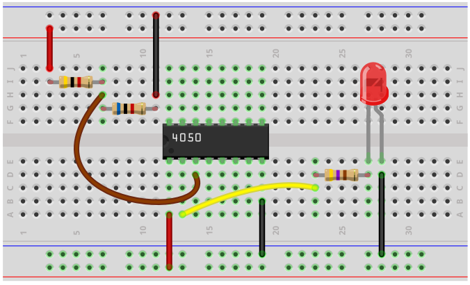
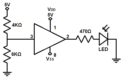
So we have our 5V power supply. However, we only want 3V. So we build a voltage divider consisting of a 4KΩ and a 6KΩ resistor. Calculating the voltage, this produces V= 5V (6KΩ/6KΩ+4KΩ)= 3V. So we will have 3V at the midway point of the 2 resistors.
If we were to add a load directly in between the resistors, the 3V wouldn't be maintained because the load has its own impedance, which may be small, so that very little voltage is allocated to it.
So the thing to do is to buffer the voltage produced from the voltage divider. We use the 4050 buffer chip to buffer the voltage from the voltage divider.
First, to power the 4050, we connect VDD, pin 1, to +5V and we connect VSS, pin 8, to ground. This establishes sufficient power for the 4050 to be able to operate.
We connect to the voltage from the voltage divider, the 3V, to the input of the first buffer of the buffer chip; this is pin 3, the input of the first buffer.
We connect the output of the this buffer to the our output load, which in this case is an LED with a current-limiting resistor as to not overpower the LED.
With a high input impedance, all the voltage from the voltage divider falls across the input of the op amp. This is because voltage, V=IR, where I is he current and R is the resistance. Being that the resistance, or impedance, is high across the input of the op amp, practically all of from the voltage divider falls across it. So, we're able to output all of the voltage to the input of the op amp.
With a low output impedance, the power isn't dragged down, so a load receives practically all of the power. If an op amp had high output impedance, it would drag down the power to such a level that current flow would be so low it couldn't power on a device. Current, I=V/R, where V is the voltage and R is the resistance. Being that current is inversely proportional to resistance, or impedance, the higher the impedance, the lower the current. For this reason, the impedance at the output must be low.
And this is how a buffer chip can be used to buffer voltage.
Related Resources
When a Circuit Needs Buffering
How to Build a Square-to-Triangle Wave Converter Circuit
How to Build a Square-to-Sine Wave Converter Circuit
How to Build a Clock Circuit with a 555 timer
How to Build an Astable Multivibrator Circuit with Transistors
How to Build a Multivibrator Circuit with a 4047 chip (for astable mode operation)
How to Build a Voltage-Controlled Oscillator Circuit with a 4046 Chip
How to Build an Oscillator Circuit with a 7414 Schmitt Trigger Inverter Chip
How to Build a Sine Wave Generator Circuit with a 555 Timer
How to Build a Ramp Generator with Transistors
How to Build a Voltage-controlled Oscillator with a 555 Timer Chip