How to Build a Register Circuit with a 74HC165 Chip
In this project, we will build a register circuit using a 74HC165 chip.
The 74HC165 register is a parallel-load, serial-out register.
What this means is this. The 74H165 is an 8-bit register. Parallel-loading means that all the 8 bits can be loaded all together at one time. This is contrast to serial loading, in which only one bit can be shifted in at a time. So parallel loading allows us to input all 8 bits together during one clock cycle, while serial loading only allows 1 bit to be shifted in during a clock cycle.
So the 74HC165 allows parallel loading on the input side and on the output side shifts bits out serially, meaning one at a time.
So, in recap, it shifts in all data at one time and shifts the data out one a time.
Parallel loading, in ways, can be viewed as simpler, because you can shift all the data in at one time.
If you connect the serial data output of a 74HC165 to a serial load, parallel output chip such as a 74HC595, you can have a parallel-in, parallel-out register. Thus, you can shift data in parallel and see the result parallel pretty much instaneously if you have a fast clock signal to the serial-in, parallel-out chip.
However, we won't build this type of circuit here.
We just simply show how a parallel-load, serial-out register works, which is what the 74HC165 chip is.
It is a serial shift register, so each bit is shifted in 1 bit at a time until all the bits are shifted in. This is in contrast to a parallel shift register, in which all 8 bits are shifted in at the same time.
The 74HC165 has 2 output pins. These are QH and
Whenever the LED at QH is on, the LED at
Even though this is not the real purpose of the circuit, it simply shows to demonstrates how the register works.
The real use of it, though, would be parallel-to-serial conversion.
Components Needed
- 74HC165 CMOS Register Chip
- 9 Pushbuttons
- 9 1KΩ resistors
- 2 470Ω resistors
- Green LED
- Red LED
- Clock source
The 74HC165 chip is a parallel-load, serial out register chip. 8 bits can be input all at once to this register.
The 74HC165 chip can be obtained very inexpensively (under $0.50) and it's available from a number of different online retailers. One place to find is at Tayda Electronics at the following link: 74HC165 CMOS Register IC.
The datasheet for the 74HC165 is shown at the following link: 74HC165 Register Datasheet.
The 74HC165 is a 16-pin chip.
The pinout for the 74HC165 is shown below.
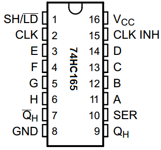
The 74HC165 works from voltage anywhere from 2V-6V. So we feed 5V into VCC, pin 16 and we connect GND to power ground.
The 8 data input pins are A-H. These are pins 11, 12, 13, 14, 6, 5, 4, and 3.
Pin 1 is the SH/
Pin 2 is the Clock (CLK) pin. A clock signal must be input into this pin in order for the register to work. Data is shifted in on the rising edge of a clock signal.
Pin 12 is the Clock Inhibit pin. We simply tie this pin LOW.
Pins 7 and 9 are the output pins. Pin 9 is QH. Pin 7 is
74HC165 Register Circuit
The schematic diagram of the 74HC165 register circuit we will build is shown below.
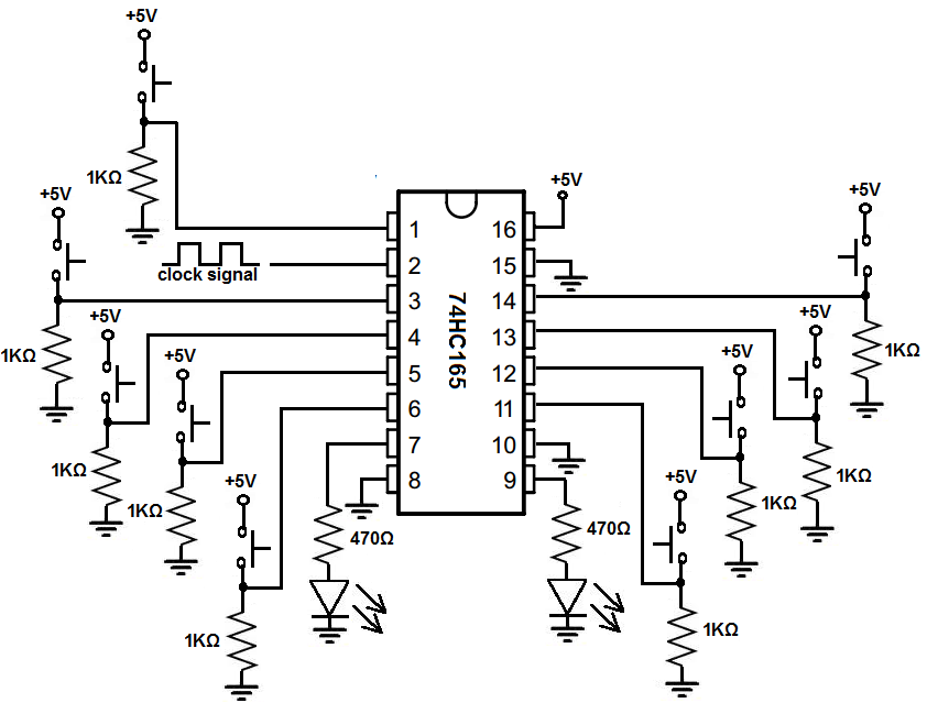
To power the 74HC165 register chip, we feed 5V into VCC, pin 16 and we connect GND to power ground. This establishes power to the 74HC165.
We connect pin 1, the SH/
To pin 2, the clock pin, we have to connect a clock signal, a digital square wave signal. This doesn't and shouldn't be a very fast signal. Anything from like 1Hz to a few KHz is sufficient. A lcok signal can be obtained from a number of sources such as from a function generator if you have one. A function generator can be put in square wave mode in which case it can function as a clock. A clock can be obtained from a 555 timer circuit in astable mode. A clock can be built with a 4047 multivibrator circuit in astable mode. A clock circuit can be built with a 7414 schmitt trigger inverter. It can also be built with a 4046 phase locked loop. So there are many ways of producing a clock signal.
To each of the data input pins, H to A, we connect a pull-down resistor. So normally, when the pushbutton is unpressed, the pin is at a LOW state. So it's a 0. If we press the pushbutton down, now the pin at a HIGH state. So it 's normally LOW when unpressed and HIGH when pressed.
We connect SER, pin 10, to ground.
We connect the Clock inhibit pin, pin 15, to ground.
To the output pins, QH and
This completes the hardware connections.
How the Circuit Works
Being that we have a clock signal, we have the CLK INH pin LOW, and we have SER LOW, the only thing else we have to do is input the data we want to on the 8 data inputs and
press down on the
SH/
The data then comes out at the QH pin, pin 9, in the order of H to A.
What you will see in this circuit is that whenever the LED at QH is on, the LED at
So it forms a toggle circuit, so to speak, as long as QH isn't all on or off.
Again, this is not the purpose of the register. The real function would be either for parallel-serial conversion of data or to form a parallel-in, parallel out circuit. But this circuit goes to show how a parallel-load, serial-out register works.
And this is how a 74HC165 register operates.
Related Resources
How to Build a Register Circuit with a 4094 Chip
How to Cascade 4094 Registers
How to Build a Shift Register Circuit with a 74HC595 Chip