How to Program an AVR chip using a USBASP
In this article, we will go over how to program an AVR chip using a USBASP.
A USBASP is a cheap device that allows for writing programs to AVR chips, such as an ATmega128 or ATmega328.
Therefore, we can write a program to blink an LED and have this program written into the flash memory of an AVR to be run, so that the LED blinks.
USBASPs are one of the least expensive options to programming AVRs; therefore, it's one of the best options for doing so. USBASPs can be obtained for under $10 on many electronic retailer sites.
It is composed of an ATmega88 or ATmega8 and a few passive components that allow for writing data to an AVR chip's flash memory.
Connecting it up to allow for it to program an AVR isn't that difficult. We will now go over the wiring connections necessary for the USBASP to transfer data from a computer to an AVR chip.
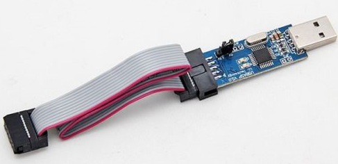
So we have the USBASP.
One end connects into the computer. This allows for us to transfer the compiled program from the computer to the USBASP. The other end of the USBASP normally gets connected either to a 6-pin or a 10-pin cable, which can then get hooked up easily to a breadboard through header pins.
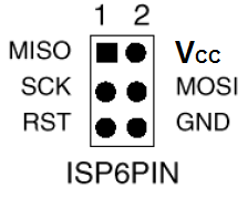
Both 6-pin and 10-pin cables are common, so knowing the pinout of these is essential to connecting them.
The 6-pin cable pinout is shown below.
This translates into the real-world wiring diagram shown below.
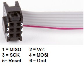
Regardless of whether the 6-pin cable or 10-pin cable is used, and it really doesn't matter, there are 6 pins we are really wiring up and these are the MISO, SCK, RST, VTG, MOSI, and GND connections.
Basically, we're connecting the USBASP to the AVR chip's MISO, SCK, RST, VTG, MOSI, and GND connections that we are programming. This allows direct communication between the USBASP and the target AVR chip.
The table below explains each of the pins and their function.
| Pin Name | Description | Comment |
| MOSI | Master Out Slave In | This allows the master device (the USBASP) to send data to the slave device (target AVR being programmed). |
| MISO | Master In Slave Out | This allows the slave device (target AVR being programmed) to send information to the master device (the USBASP programmer). |
| SCK | Serial Clock | This is the mutual clock shared between the master and slave device for synchronized communication. |
| Reset | Target AVR MCU Reset | The reset pin for the AVR chip being programmed must be put in active low in order for programming to occur. |
| Vcc | Power | The master and slave device both need power in order to operate. |
| GND | Common Ground | The master and slave device must share a common power ground. for operation. |
With this setup, the USBASP is the master device and the AVR chip we are programming is the target, or slave device. The best way to think of it is the master device is doing the programming, while the slave device is the subordinate device that is need of being programmed.
In order for a master device to program a slave device, they need have communication amongst each other. The master device needs to be able to write data to the slave device's flash memory and be able to receive data from the slave data. This is done through the MOSI and MISO pins. The MOSI pin stands for Master Out Slave In. This is the pin by which the master device outputs, or writes, data to the target AVR which is being programmed. MISO stands for Master In Slave Out. This is the pin by which the slave device (AVR being programmed) can send information to the master device. Both these communication pathways are essential to program a device. So the MOSI and MISO pins establish communcation amongs the master device and the slave device it is to program.
The SCK pin is the clock. It is essential because in order for the master and slave device to communicate, they need to have a time signal to communicate data in synchrony. The common clock signal shared between the master and slave device allow for efficient communication.
The RST pin is an essential connection because it must be put to an active low connection in order for programming to occur between the master and slave device. It is normally held high, but for programming to occur, it must be put low. It is an active low pin. When the RST pin is put low, the master slave can communicate on the SCK, MISO, and MOSI lines.
The remaining 2 connections, VCC and GND, are the simplest; they are for power. The AVR chip being programmed and the master device doing the programming both need to power in order to operate.
These are the only 6 essential connections that need to be made from the USBASP Programmer to the target AVR chip.
Using the popular ATmega328 chip as an example, we will show the wiring necessary to connect a USBASP to an Atmega328 chip to program it.
The schematic diagram for wiring the USBASP to the Atmega328 chip is shown below.
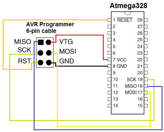
Basically, we just have to know which pins are the MOSI, MISO, SCK, RST, VCC, and GND pins, and connect
them correspondingly from the USBASP to the target AVR chip.
And with these 6 connections we can program AVR chips.
Related Resources
How to Use the LM741 Op Amp as a Comparator
How to Build an LM339 Quad Voltage Comparator Circuit
How to Build a Dark-activated Switch
How to Build a Hall Effect Sensor Circuit
How to Build a Touch Sensor Circuit
How to Build an Accelerometer Circuit
How to Build a Motion Detector Circuit
How to Build a Motion Detector Alarm Circuit