
How to Build a Switch Mode Power Supply Circuit with an MC34063
In this project, we will show how to build a switch mode power supply circuit with a MC34063 chip. A switch mode power supply is also called a switched mode power supply or a switching mode power supply.
A switch mode power supply is a power supply that regulates a certain power output. A switch mode power supply switches on and off to keep the desired voltage output. It switches on when the power is below the desired output and once the power output is above the desired output it switches off. Therefore, the voltage gets a little above the desired voltage output and a little below the desired output voltage, but it's negligible how little it varies from the desired voltage output range. It pretty much stays right on course of the desired voltage output.
By switching on and off, the switching mode power supply can obtain a much higher power efficiency than a linear power supply. A linear power supply does not switch on and off. It has a continuous flow of power into it. Therefore, it's less efficient than a switching mode power supply which is off for periods of time. When the switch mode power supply is completely off, it is using no power at all during these times. switch mode power supplies can obtain efficiencies of over 90%. Linear power supplies can have horrible power efficiencies. Let's use the example of us using a linear power supply of a 9V and we want 5V output. This is a power efficiency of, power efficiency= (power output/power ) * 100%= (5V/9V) * 100, which is a power efficiency of 55%. This means we are wasting 45% of the power supplied to the circuit. This is a huge waste. Well-designed swithced mode power supplies can achieve much greater efficiencies. This is the advantage of switch mode power supplies. It offers greater power efficiencies and, thus, less wasted power. For one, a pulse or square waveform is fed into a switch mode power supply. As said before, a switch mode power supply does not use continuous power. It uses on-and-off power, a square wave or a pwm wave. It makes it more power efficient because at the off times of each cycle, the circuit isn't even using any power at all. A linear power supply, on the other hand, uses continous power that is always on.
We'll go over in more detail how a switch mode power supply works and is able to sustain a continuous power output, even while the input power is off for a period of time.
We show how to build the circuit below.
And even though a switch mode power supply offers increased power efficiency,
Components Needed
- MC34063 Regulator Chip
- 1KΩ resistor
- 7KΩ resistor
- 180Ω resistor
- 270pF ceramic capacitor
- 39μH inductor
- 2 100μF electrolytic capacitor
The MC34063 is a very versatile chip. It is a DC-DC converter chip that can be used as a buck converter, a boost converter, or an inverter. So it can function as a step-up converter, a step-down converter, or an inverter with a combination of step-up or step-down function.
It is used in many types of devices in order to regulate voltages and it is very common. It is used in everyday devices such as car chargers for instance to regulate voltage levels. So it's an industry-standard device. It's created by a host of different electronic manufacturers, so it can be obtained very cheaply.
The MC34063 has can operate on an input voltage of 3V-40V. It has output switch curren capability of up to 1.5A. The output voltage is adjustable. And it can switch power at frequencies up to 100KHz.
The datasheet for the MC34063 chip can be found at the following link: MC34063 Switching Regulator Datasheet.
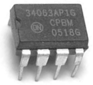
It's an 8-pin chip.
The pinout of the chip is shown below.
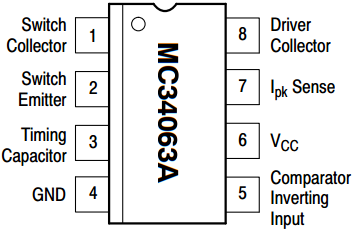
Pin 1 is the switch collector and pin 8 is the drive collector in the chip. These pins are the collectors of the 2 internal transistors in the chip. The switching power supply works through saturating a transistor at various intervals. Through saturating a transistor at repeat intervals, a power level can be achieved at desired levels. Unlike a linear power supply, in which the transistor is always saturated, in a switching power supply, the power supply is only saturated at certain time intervals and off during others. This allows for more efficient use of power and less power waste. So these pins of the collectors of this periodic transistor saturation.
Pin 2 is the emitter of both of the switch and drive transistors. It simply connects to ground.
Pin 3 is the timing capacitor chip. To this pin, a capacitor is connected that determines the switching speed of the circuit.
Pin 4 is the ground of the reference voltage regulator. Inside the MC34063 is a reference regulator that inputs 1.25V into a comparator inside the chip. This comparator allows us to determine the gain of the output voltage by the formula, VOUT= 1.25V (1 + R2/R1. More is explained about this in depth below. But since this pin is the ground of the reference voltage regulator, we simply connect it to ground.
Pin 5 is the comparator inverting input terminal. To the noninverting terminal is the 1.25V input from the 1.25 reference voltage regulator. To the inverting terminal, we connect a resistor network that allows us to determine the output voltage gain. So this this pin, we will connect 2 resistors, R1 and R2 that allows us to decide what the gain of the circuit will be.
Pin 6 is the power pin, VCC. To this pin, we connect our positive voltage supply. The pin can operate from 3V to 40V of power. So we can input this range of voltage to this pin. From this voltage, the chip uses power for the internal transistors, comparator, as well as other components. So the power inserted into VCC runs a lot internally for the chip.
Pin 7 is the IPK pin. It holds the maximum current that runs through the transistor, which will run through the inductor and diode, since they are connected to the output of the transistor. To this pin, we place a resistor that we calculate based on a a formula from the datasheet. This resistor sets the maximum current.
For the diode, we use a 1N5819 diode, which is a schottky barrier rectifier diode. It is used because it has a lower voltage drop than a silicion diode, so it's more power efficient for this circuit.
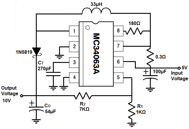
In this circuit, we're going to use the MC34063 chip in step-up mode so that it boosts the voltage that we supply it.
We're going to step up 5V to 10V with a current output of 100mA.
The MC34063 datasheet has example circuits for the 3 modes of the chip: step-up, step-down, and inverter.
If you look at the example circuit of the MC34063 circuit in step-up mode, it converts 12V to 28V. This is a bit high of a voltage to deal with. Therefore, in our circuit, we tone it down and make it the input voltage 5V and the output voltage 10V.
In order to bias our circuit and get the output voltage that we want for the input voltage that we put in, we can need to calculate several values for our circuit.
Switch Mode Power Supply Circuit built with an MC34063 Chip
The switch mode power supply circuit that we will build with an
MC34063 chip is shown below.
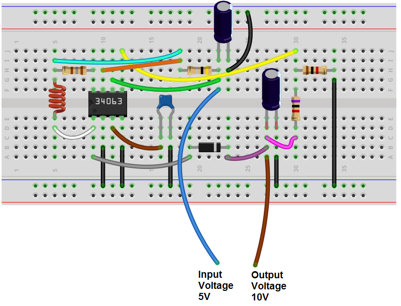
The breadboard circuit of the circuit above is shown below.
So the circuits are shown above. How we calculated most of the values of the components of each of the parts of the circuits are through the formulas on the data.
On the datasheet for the MC34063, there are a bunch of formulas there for the calculations we need to do.
We will go through each and every one of them so that we can have as much control over our circuit as possible. These formulas will determine the values of the external inductors, resistors, and capacitors used in the circuit, so it must be done.
TON/TOFF= (VOUT + VF - VIN (MIN))/ (VIN (MIN) - VSAT)= (15V + 0.4V - 4.5V)/(4.5V - 0.45V)≈ 1.5μs.
VOUT is the voltage that we want output, which is 10V. We are trying to convert the 5V input into 15V output.
VF is the voltage drop of the diode that you are using. You may have to consult the datasheet for the diode you are using. This value usually doesn't vary too much and won't be too critical because it is such a small value, so it doesn't hold that much weight in the equation.
VIN (MIN) is the minimum voltage that VIN can be. Being that we want VIN to be 5V, we will use this value as VIN (MIN).
VSAT is the saturation voltage of the internal transistor in the chip. To find the value of the saturation voltage, you need to consult the datasheet. If you go to the electrical characteristics table in the datasheet, there are 2 saturation voltages listed. The first saturation voltage, with the darlington connection, applies to step-down circuits. Therefore, it doesn't apply here. It is the second saturation voltage that we use. Looking to the right, the typical saturation voltage is 0.45V. Therefore, this is the value we use in our calculation.
The next equation calculates the time period of the input signal.
TON + TOFF = 1/f= 1/100KHz= 10μs. We will use the maximum 100KHz allowed, because the faster the switching speed of the circuit, the lower the inductance has to be in the circuit. In this circuit, we are using an inductor in the microhenry range. We don't want to have to use a very large inductor that can't be obtained. To offset this, we use the highest possible frequency possible. The faster the circuit swiches on and off, the less the need for a greater inductance.
To calculate TOFF, we use the formula, TOFF= (TON + TOFF)/(TON/TOFF + 1)= 10μs/2.7μs +1= 4μs.
To calculate TON, we use the formula, (TON + TOFF) - TOFF= 10μs - 4μs= 6μs.
Next we calculate the value of the external capacitor that connects to pin 3 that sets the switching frequency. The capacitor, CT= 4 * 10-5 * TON= 4 * 10-5 * 6μs= 240pF.
IPK is the peak current that flows through the inductor and the diode. IPK is 2 * IO (MAX) * (TON/TOFF + 1) = 2 * 0.1 * (3.3μs + 1)= 0.86A. So since 0.86A is the peak current that flows through both the inductor and the diode, both these components need to be rated for current peaks above this value. For example, a 1A rating on both of these components will suffice, but it can't be under this value, or else the components can get destroyed from excess current. Therefore, it's very important to check the current specs for each of these components before putting them in the circuit.
RSC is the sense current resistor. RSC= 0.3/IPK = 0.3/0.86A= 0.3 ohms.
LMIN is the minimum value the inductor should be for our circuit.
LMIN= (VIN (MIN) -VSAT)/IPK * TON= (5V- 0.45V)/0.86A * 6μs= 31.7μH. So 31.7μH is the value of the inductor we will use in the circuit.
CO is the, output or filter capacitor used for our circuit. We use 3 capacitors in our circuit. One is to configure the switching frequency. The other 2 act as filter capacitors so that we don't get excess noise on the input signal or excess ripple on the output signal.
CO= 9 * (IOUT * TON)/VRIPPLE= 9 * (0.1 * 6μs/0.1)= 54μF. This is the output capacitor we need.
The last thing we need to calculate, which is very important are the resistor values that determine the voltage output. This circuit functions just as an op amp gain circuit.
The formula for VOUT= 1.25 (1 + R2/R1). Since we want an output voltage of 9V, let's first choose a generic value for R1KΩ for R1. Since R1=1KΩ, R2 has to equal to 6.2KΩ in order to equal 9V. Doing the math, we get, VOUT= 1.25 (1 + R2/R1)= 1.25 (1 + (7KΩ/1KΩ))= 10V. Choosing the R1 and R2 resistors is actually really neat because this part of the circuit determines the gain or amplitude of our output signal. This part of the circuit is a noninverting op ap circuit. So its gain is the same as noninverting input gain. The reference voltage at the noninverting terminal is 1.25V, so this is why you see 1.25V in this equation. It is the reference voltage. Whatever voltage is fed into the noninverting terminal is the reference voltage. This voltage gets multipled by 1 + R2/R1 to get the final voltage output.
You can change this to whatever voltage you want.
If you want 9V, then R2 should be 6.2 times the voltage of R1.
If you want 12V, then R2 should be 8.6 times the voltage of R1.
If you want 15V, then R2 should be 11 times the voltage of R1.
It's pretty basic math how to calculate the gain. Just think whatever voltage you want, is going to want as output, first divide that number by 1.25, then subtract 1. The remaining number is R2/R1. Whatever that value is gets multipled by the R1 resistor to get R2. And that's all. It's really that simple.
And these are all the calculations that need to be computed for this circuit.
So from these formulas, we find the value of all the components we need.
Realize that you may not find the exact component values of those which we need.
It may be hard to find a 0.3Ω resistor, so instead you can use a 1Ω resistor or take 2 1Ω resistors and place them in parallel which will give about 0.5Ω of resistance. 1Ω resistors are readily available.
31.7μH inductors aren't readily available, so you can approximate and use 33μH inductors, which are readily avaiable.
54μF capacitors are not readily available, so you can just round up and use a readily available 100μF capacitor, which is definitely easier.
240pF won't be avaiable, so you can use a 270pF capacitor in place.
And 180Ω resistors are easily obtainable. This 180Ω resistor does not need to be calculated.
It's simply taken directly from the datasheet. Neither does the 100μF capacitor connected at the input
voltage. This is just a generic capacitor that functions to remove ripple and noise from the input voltage.
Connecting the Circuit
So we have our MC34063 chip. To power this chip, we connect +5V to VCC, pin 6, and we connect the pin 4 to ground. This establishes power for the chip. Internally, there are a lot of components in the chip that need power, including transistors and comparators. After the input voltage, to VCC, we connect a 100μF capacitor, which acts as a filter capacitor so that excess noise from the power supply is filtered out.
Pin 2 is the emitters of the 2 internal transistors, so pin 2 is connected to ground.
Pin 3 is the timing capacitor. It determines the switching speed of the circuit.
Pin 5 is inverting terminal of the comparator. The noninverting terminal is fed 1.25V from the internal voltage regulator. To the inverting terminal, we place a resistor network composed of 2 resistors. These decide the gain of the op amp comparator by the formula, VOUT= 1.25V (1 + R2/R1). Since we want an output voltage of 10V, R1= 1KΩ and R2= 7KΩ.
Pin 7 is the IPK sense pin. To this pin, we connect a 0.4Ω resistor based on our calculations. Like stated above, if 2 1Ω resistors can be placed in parallel to give a voltage near this level.
Pin 1 and 8 are the collectors of the 2 transistors internally inside the chip. An inductor is connected in between these 2 collectors. So the output of the transistors goes and charges up the inductor when saturated. When turned off, the inductor discharges and charges up capacitor CO, the output capacitor, through the diode. This is how the circuit has its boost functionality. The inductor stores charge and creates a magnetic field. Once the transistor is off and current stops flowing through the inductor, the charge from the inductor discharges through the diode and charges up the capacitor. This charging up takes place multiple times until the capacitor reaches the peak voltage intended based on the gain that the circuit is designed to reach.
Since we are choosing 10V for the output capacitor, the capacitor must be rated at least for this voltage. If you are designing your circuit for even a greater voltage gain, take into account that the capacitors must be rated for the voltages they are exposed to. This applies for the capacitor at the input and the one at the output.
And this is a classic switch mode power supply using the MC34063 chip to act as a step-up
or boost converter.
Related Resources
How to Build a Square-to-Triangle Wave Converter Circuit
How to Build a Square-to-Sine Wave Converter Circuit
How to Build a Clock Circuit with a 555 timer
How to Build an Astable Multivibrator Circuit with Transistors
How to Build a Multivibrator Circuit with a 4047 chip (for astable mode operation)
How to Build a Voltage-Controlled Oscillator Circuit with a 4046 Chip
How to Build an Oscillator Circuit with a 7414 Schmitt Trigger Inverter Chip
How to Build a Sine Wave Generator Circuit with a 555 Timer
How to Build a Ramp Generator with Transistors
How to Build a Voltage-controlled Oscillator with a 555 Timer Chip